Cirrus Logic CS4362A User Manual
Cs4362a, Channel d/a converter, Features
Copyright
© Cirrus Logic, Inc. 2009
(All Rights Reserved)
114 dB, 192 kHz
6
-Channel D/A Converter
Features
Advanced Multi-bit Delta Sigma Architecture
24-bit Conversion
Up to 192 kHz Sample Rates
114 dB Dynamic Range
-100 dB THD+N
Direct Stream Digital
®
(DSD
™
) Mode
On-chip 50 kHz Filter
Matched PCM and DSD Analog Output Levels
Selectable Digital Filters
Volume Control with 1 dB Step Size and Soft
Ramp
Low Clock-jitter Sensitivity
+5 V Analog Supply, +2.5 V Digital Supply
Separate 1.8 to 5 V Logic Supplies for the
Control & Serial Ports
Description
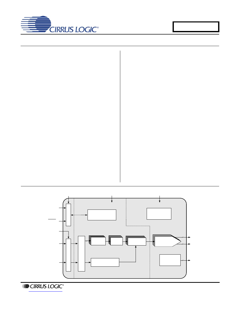
The CS4362A is a complete 6-channel digital-to-analog
system. This D/A system includes digital de-emphasis,
1 dB step size volume control, ATAPI channel mixing,
selectable fast and slow digital interpolation filters fol-
lowed by an oversampled, multi-bit delta-sigma
modulator which includes mismatch shaping technolo-
gy that eliminates distortion due to capacitor mismatch.
Following this stage is a multi-element switched capac-
itor stage and low-pass filter with differential analog
outputs.
The CS4362A also has a proprietary DSD processor
which allows for 50 kHz on-chip filtering without an in-
termediate decimation stage. The CS4362A is available
in a 48-pin LQFP package in both Commercial (-40°C to
+85°C) and Automotive grades (-40°C to +105°C). The
CDB4362A Customer Demonstration board is also
available for device evaluation and implementation sug-
gestions. Please see
“Ordering Information” on page 48
for complete details.
The CS4362A accepts PCM data at sample rates from
4 kHz to 216 kHz, DSD audio data, and delivers excel-
lent sound quality. These features are ideal for multi-
channel audio systems including SACD players, A/V re-
ceivers, digital TV’s, mixing consoles, effects
processors, sound cards, and automotive audio
systems.
Control Port Supply = 1.8 V to 5 V
Register/Hardware
Configuration
Internal Voltage
Reference
Reset
S
e
ri
a
l Inte
rface
L
e
ve
l Tr
ans
lato
r
L
e
vel Translato
r
Digital Supply = 2.5 V
Hardware Mode or
I
2
C/SPI Software Mode
Control Data
Analog Supply = 5 V
Six Channels of
Differential
Outputs
PCM Serial
Audio Input
Volume
Controls
Digital
Filters
Switch-Cap
DAC and
Analog Filters
Multi-bit
∆Σ
Modulators
DSD Audio
Input
DSD Processor
-50 kHz filter
External Mute
Control
Mute Signals
Serial Audio Port
Supply = 1.8 V to 5 V
6
6
6
6
CS4362A
JAN '09
DS617F2
Document Outline
- 1. Pin Description
- 2. Characteristics and Specifications
- Recommended Operating Conditions
- Absolute Maximum Ratings
- DAC Analog Characteristics - Commercial (-CQZ)
- DAC Analog Characteristics - Automotive (-DQZ)
- Power and Thermal Characteristics
- Combined Interpolation & On-Chip Analog Filter Response
- Combined Interpolation & On-Chip Analog Filter Response
- DSD Combined Digital & On-chip Analog Filter Response
- Digital Characteristics
- Switching Characteristics - PCM
- Switching Characteristics - DSD
- Switching Characteristics - Control Port - I·C Format
- Switching Characteristics - Control Port - SPI Format
- 3. Typical Connection Diagram
- 4. Applications
- 4.1 Master Clock
- 4.2 Mode Select
- 4.3 Digital Interface Formats
- 4.4 Oversampling Modes
- 4.5 Interpolation Filter
- 4.6 De-emphasis
- 4.7 ATAPI Specification
- 4.8 Direct Stream Digital (DSD) Mode
- 4.9 Grounding and Power Supply Arrangements
- 4.10 Analog Output and Filtering
- 4.11 Mute Control
- 4.12 Recommended Power-Up Sequence
- 4.13 Recommended Procedure for Switching Operational Modes
- 4.14 Control Port Interface
- 4.15 Memory Address Pointer (MAP)
- 4.16 INCR (Auto Map Increment Enable)
- 5. Register Quick Reference
- 6. Register Description
- 6.1 Mode Control 1 (Address 01h)
- 6.2 Mode Control 2 (Address 02h)
- 6.3 Mode Control 3 (Address 03h)
- 6.4 Filter Control (Address 04h)
- 6.5 Invert Control (Address 05h)
- 6.6 Mixing Control Pair 1 (Channels A1 & B1)(Address 06h) Mixing Control Pair 2 (Channels A2 & B2)(Address 09h) Mixing Control Pair 3 (Channels A3 & B3)(Address 0Ch)
- 6.7 Volume Control (Addresses 07h, 08h, 0Ah, 0Bh, 0Dh, 0Eh)
- 6.8 Chip Revision (Address 12h)
- 7. Filter Plots
- 8. Parameter Definitions
- 9. Package Dimensions
- 10. Ordering Information
- 11. References
- 12. Revision History