8 power supply circuitry, 9 grounding and power supply decoupling, Table 1 – Cirrus Logic CDB4207 User Manual
Page 5: Cdb4207
CDB4207
DS880DB1
5
1.8
Power Supply Circuitry
The CDB4207 has several options for powering the CS4207 and auxiliary circuits. The main board power
supply can be used to power the entire board through on-board regulators. The main board power supply
can be provided by pin 10 of the HD Audio Bus header J1/J9, the PC peripheral power supply connector
J14, or an external bench supply using J8 and J7. The three options are separated via Schottky diodes, thus
the applied source with the largest voltage will be used. To use only this single power source, the CS4207
supply source selection headers (J10, J11, J12, J13, and J15) should be shunted in the ‘REG’ positions.
Alternatively each CS4207 supply can be sourced directly from external bench supplies via banana jacks
by shunting the ‘EXT’ position. In this case the main board power supply is still required to regulate a +3.3 V
supply for the S/PDIF optical jacks, the digital microphone power, and the GPIO pull-up resistors.
For the VL_HD supply ‘REG’ setting, J19 selects whether the supply is +3.3 V (unshunted) or +1.5 V (shunt-
ed). For the VD supply ‘REG’ setting, J18 selects whether the supply is +1.8 V (unshunted) or +1.5 V (shunt-
ed). For the VA supply ‘REG’ setting, J17 selects whether the supply is +5 V (unshunted), +4.7 V (1-2
shunted), +3.3 V (3-4 shunted), or +3.1V (5-6 shunted). In addition to the regulator and external options, the
CS4207’s VL_IF and VL_HD supplies can be powered directly from 3.3V_DVDD_CORE and DVDD_IO on
J1/J9 (‘HDA’), respectively, and the VA_HP supply can be powered directly from 3.3V_DVDD_CORE on
J1/J9 (‘3.3 V HDA’) or +5 V on J14 (‘5.0 V HDD’).
Note that the VL_HD supply voltage must match the chipset voltage used by the connected PC. This con-
dition is guaranteed when the ‘HDA’ setting on J12 is selected instead of ‘REG’ or ‘EXT’.
There are nine power supply indicator LEDs on the CDB4207. Each LED will be lit whenever the associated
supply is turned on. See
for the power supply circuit schematic and
for the power supply connections, jumper selections, and indicator LEDs.
1.9
Grounding and Power Supply Decoupling
As with any high-performance converter, the CS4207 requires careful attention to power supply and ground-
ing arrangements to optimize performance.
details the connections to the CS4207 and
,
, and
show the component placement and the board layout. The decoupling capacitors are locat-
ed as close as possible to the CS4207.
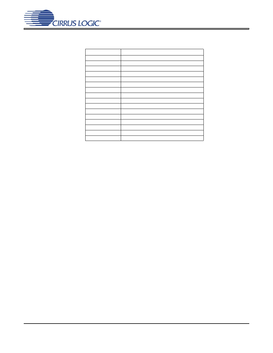
Table 1. CDB4207 HD Audio Bus Header Pinout (J1 and J9)
Pin
Signal
1
BCLK
2
GND
3
RST#
4
DVDD_IO (to J12 VL_HD header)
5
SYNC
6
GND
7
SDO
8
3.3V_DVDD_CORE (to J13 VL_IF header)
9
SDI0
10
+12V
11
SDI1
12
Key (no connection)
13
SDI2
14
3.3V_DUAL (to D12 indicator LED)
15
SDI3
16
GND