Pin description, Figure 6. cs3302a pin assignments, Table 2. pin descriptions – Cirrus Logic CS3302A User Manual
Page 14: Cs3302a
CS3302A
CS3302A
DS765PP1
14
DS765PP1
3.
PIN DESCRIPTION
Pin Name
Pin #
I/O
Pin Description
VA+
1
I
Positive analog supply voltage.
VA-
4
I
Negative analog supply voltage.
VD
16
I
Positive digital supply voltage.
GND
15, 18
I
Ground.
INA+, INA-
5, 6
I
Channel A differential analog inputs. Selected via MUX pins.
INB+, INB-
8, 7
I
Channel B differential analog inputs. Selected via MUX pins.
GUARD
13
O
Guard voltage output.
OUTR+, OUTR-
11, 2
O
Rough charge differential analog outputs.
OUTF+, OUTF-
10, 3
O
Fine charge differential analog outputs.
GAIN0, GAIN1,
GAIN2
22, 21,
20
I
Gain range select. See Gain Selection table in Digital Characteristics section.
PWDN
19
I
Power down mode enable. Active high.
MUX0, MUX1
24, 23
I
Analog input select. See Input Selection table in Digital Characteristics section.
TEST0
12
I
Test mode select, factory use only. Connect to VA- during normal operation.
TEST1, TEST2
17, 14
I
Test mode select, factory use only. Connect to GND during normal operation.
TESTOUT
9
O
Test mode output, factory use only. Do not connect during normal operation.
Table 2. Pin Descriptions
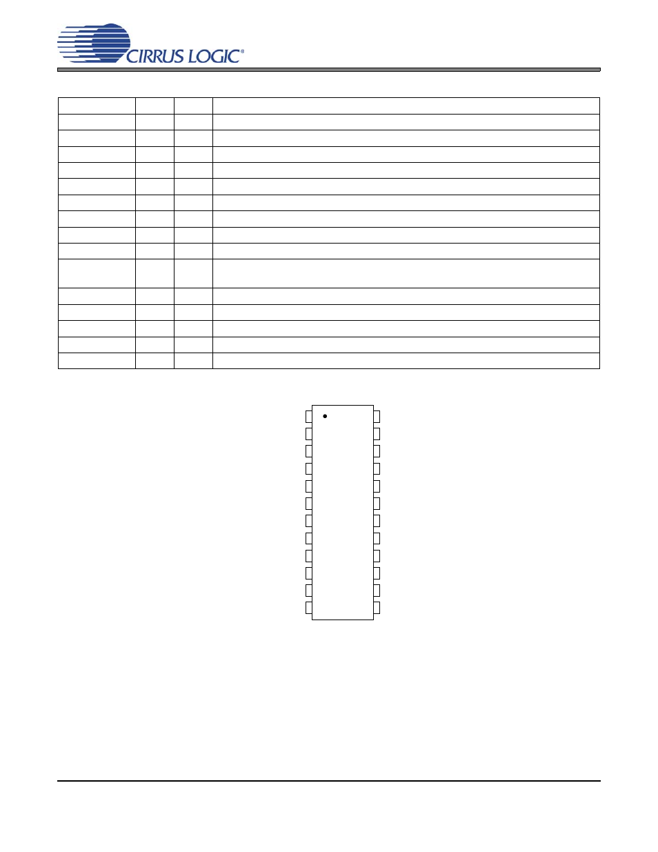
1
2
3
4
5
6
7
8
17
18
19
20
21
22
23
24
9
10
11
12
13
14
15
16
Positive Analog Power Supply
VA+
Negative Analog Rough Output
OUTR-
Negative Analog Fine Output
OUTF-
Negative Analog Power Supply
VA-
Non-Inverting Input A
INA+
Inverting Input A
INA-
Inverting Input B
INB-
Non-Inverting Input B
INB+
Test Mode Output
TESTOUT
Positive Analog Fine Output
OUTF+
Positive Analog Rough Output
OUTR+
Test Mode Select
TEST0
MUX0
Input Mux Select
MUX1
Input Mux Select
GAIN0
Gain Range Select
GAIN1
Gain Range Select
GAIN2
Gain Range Select
PWDN
Power Down Mode Enable
GND
Ground
TEST1
Test Mode Select
VD
Positive Digital Power Supply
GND
Ground
TEST2
Test Mode Select
GUARD
Guard Voltage Output
Figure 6. CS3302A Pin Assignments