3 design process, An375, Figure 2 – Cirrus Logic AN375 User Manual
Page 5: Buck-boost model
AN375
AN375REV4
5
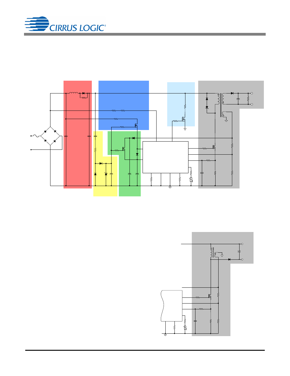
3 Design Process
The design process for a single-stage power converter system can be partitioned into six circuit blocks (see
Figure 1). The AC line voltage is rectified, then passed through an electromagnetic interference (EMI) filter to sup-
press conducted interference generated by the circuit on the power line. The output of the EMI filter is then converted
to the desired DC output by a dual-mode flyback/buck-boost converter. The power converter system includes the
gate bias, steady state supply, and active clamp support circuitry.
The CS1615/16 is configurable for isolated or non-isolated topologies using a flyback transformer or buck-boost in-
ductor, respectively. Figure 1 illustrates the dual-mode flyback topology. The CS1615/16 regulates output current
using primary-side control, which eliminates the need for opto-coupler feedback.
The CS1615/16 controls the dual-mode flyback/buck-
boost to satisfy the dimmer hold current requirement in
Dimmer Mode and provide power factor correction in
No-dimmer Mode. Figure 2 illustrates the dual-mode
buck-boost topology. The CS1615/16 regulates the output
current by controlling the peak current to ensure that the
target output charge is achieved every half line-cycle. The
dual-mode ensures a minimum average input current
greater than the required dimmer hold current when be-
hind a dimmer and shapes the line current when not be-
hind a dimmer to provide power factor correction.
The dual-mode buck-boost is simulated using a transform-
er with a turns ratio of one. Demagnetization time of the
transformer/inductor is sensed by the FBAUX pin using an
auxiliary winding and is used as an input to the control
loop.
EMI
Dimmer Compatibility
Gate Bias
Steady State
Supply
Flyback
L2
LED +
NTC
C7
R18
LED -
CS1615/16
FBAUX
SGND
IAC
GD
VDD
SOURCE
eOTP
FBSENSE
GND
CTRL1
CTRL2
BR1
F1
L
N
AC Line
Voltage
R3
C11
Q4
R20
R7
R8
R10
R23
R13
R17
L1
C4
R5
D7
R6
R19
C13
Z1
D4
D4
R4
C6
C2
Q2
R2
Q1
R1
D3
C1
D6
C10
D1
R15
Q3
R21
R16
Active Clamp
(Optional)
CLAMP
D5
Z2
V
rect
Figure 1. Block Diagram of CS1615/16 Design
NTC
C7
R18
CS1615/16
FBAUX
GD
eOTP
FBSENSE
GND
CTRL2
Q4
R20
R10
R23
R17
R6
R19
LED-
L2
D7
C4
Buck-boost
LED +
V
rect
V
AUX
Figure 2.
Buck-boost Model