2 switch overpower protection, 4 voltage clamp circuit, 1 clamp overpower protection – Cirrus Logic CS1616 User Manual
Page 9: 6 dual-mode flyback / buck-boost, 6 dual-mode flyback/buck-boost, Figure 12. clamp pin model, Figure 13. flyback model
CS1615/16
DS961F1
9
dimmer switch on the falling edge of the input voltage using a
source-controlled dimmer-compatibility circuit.
5.3.2 Switch Overpower Protection
To prevent excessive power dissipation on the source-switched
FET Q1, the CS1615/16 monitors voltage across FET Q1 and
current flow through FET Q1 to calculate average power
dissipation. If the calculated power exceeds the overpower
protection threshold a fault condition occurs. The IC output is
disabled and the controller attempts to restart after
approximately thirty seconds.
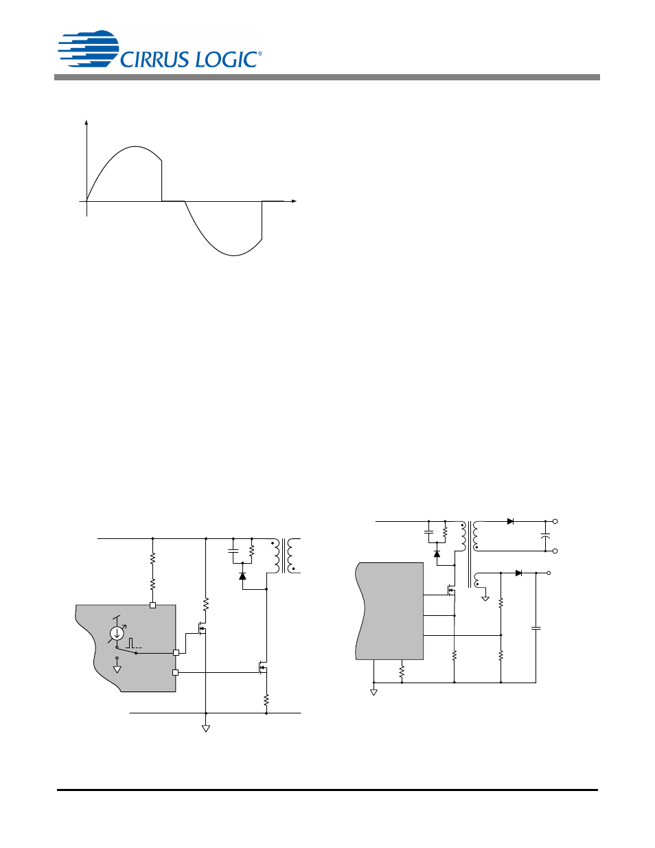
5.4 Voltage Clamp Circuit
To keep trailing-edge dimmer switches conducting and from
misfiring, the dimmer switch internal capacitor has to be
charged quickly around the trailing edge of the phase-cut
waveform. In addition to the dimmer compatible circuit, an
optional clamp circuit provides a high-current sinking path for
delivering the required amount of charge onto the dimmer
switch capacitor in a short amount of time.
The CS1615/16 provides active clamp circuitry on the CLAMP
pin, as shown in Figure 12.
5.4.1 Clamp Overpower Protection
The CS1615/16 clamp overpower protection (COP) control logic
averages the turn-on time of the clamp circuit. If the output of the
averaging logic exceeds 10%, a COP event is actuated. The
clamp circuit is disabled as well as the flyback/buck-boost
controller and the dimmer-compatibility circuit. The COP fault
state is not cleared until the power to the IC is recycled.
5.5 Dimmer Angle Extraction and the Dim
Mapping Algorithm
When operating with a dimmer, the dimming signal is extracted
in the time domain and is proportional to the conduction angle of
the dimmer. A control variable is passed to the quasi-resonant
flyback/buck-boost controller to achieve a wide range of output
currents.
5.6 Dual-mode Flyback/Buck-boost
The CS1615/16 is configurable for isolated or non-isolated
topologies using a flyback transformer or buck-boost inductor,
respectively. The CS1615/16 controls the dual-mode
flyback/buck-boost to satisfy the dimmer hold current
requirement in Dimmer Mode and provide power factor
correction in No-dimmer Mode. The dual-mode ensures a
minimum average input current greater than the required dimmer
hold current when behind a dimmer and shapes the line current
when not behind a dimmer to provide power factor correction. It
also ensures half line-cycle averaged constant output current.
Figure 13 illustrates the dual-mode flyback topology. The
CS1615/16 regulates output current using primary-side control,
which eliminates the need for opto-coupler feedback. The control
loop operates in peak current control mode. Demagnetization
time of the transformer is sensed by the FBAUX pin using an
auxiliary winding and is used as an input to the control loop.
Figure 11. Trailing-edge Mode Phase-cut Waveform
CLAMP
R
Clam p
I
CLAM P
V
rect
S1
CS1615/16
VDD
Q
T1
R4
D3
R6
C6
R5
Q3
R
Sense
3
13
GD
2
IAC
Figure 12. CLAMP Pin Model
R
CTRL2
CTRL2
FBAUX
GND
GD
9
12
CS1615/16
16
13
T1
D3
R6
C6
Q3
R
S ense
V
rect
FBSENSE 11
C7
LED+
LED-
R7
C8
R8
V
AUX
D5
D4
Figure 13. Flyback Model