Pin description – Cirrus Logic CS1616 User Manual
Page 3

CS1615/16
DS961F1
3
2. PIN DESCRIPTION
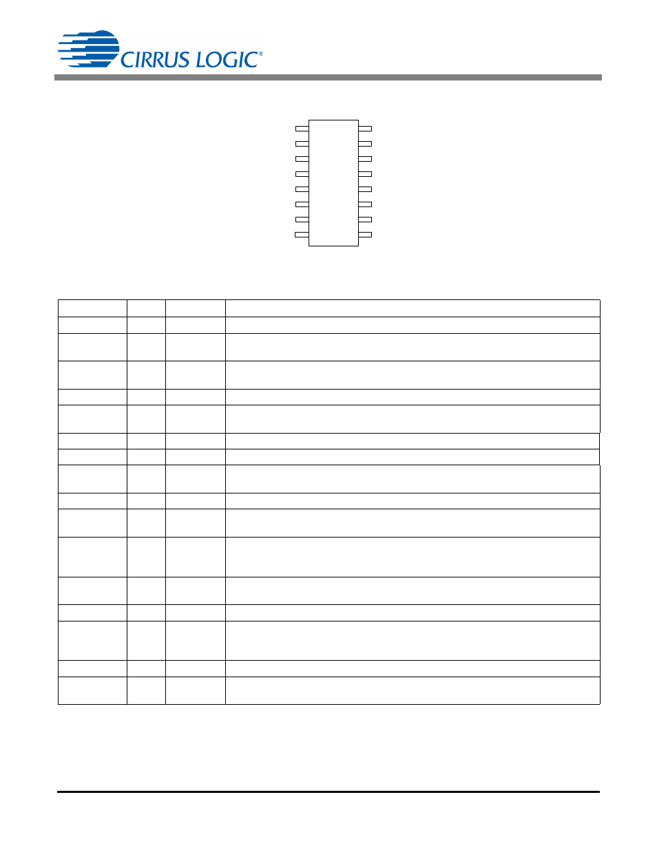
Figure 2. CS1615/16 Pin Assignments
16-lead SOIC and TSSOP
16
Zero-current Detect
FBAUX
15
No Connect
NC
14
IC Supply Voltage
VDD
13
GD
Gate Drive
10
eOTP
External Overtemperature Protection
11
FBSENSE
Flyback Current Sense
12
GND
Ground
9
LED Load Current
CTRL2
No Connect
NC
1
2
IAC
Rectifier Voltage Sense
3
Voltage Clamp Current Source
CLAMP
4
SGND
Source Ground
5
Source Switch
SOURCE
6
NC
No Connect
7
No Connect
NC
8
CTRL1
Dimmer Hold Current
Pin Name
Pin #
I/O
Description
NC
1
IN
No Connect — Leave pin unconnected.
IAC
2
IN
Rectifier Voltage Sense — A current proportional to the rectified line voltage is fed
into this pin. The current is measured with an A/D converter.
CLAMP
3
OUT
Voltage Clamp Current Source — Connect to a voltage clamp circuit on the
source-switched dimmer-compatibility circuit.
SGND
4
PWR
Source Ground — Common reference current return for the SOURCE pin.
SOURCE
5
IN
Source Switch — Connected to the source of the source-switched external high-volt-
age FET.
NC
6
IN
No Connect — Connect this pin to VDD using a 47k
pull-up resistor.
NC
7
IN
No Connect — Connect this pin to VDD using a 47k
pull-up resistor.
CTRL1
8
IN
Dimmer Hold Current — Connect a resistor to this pin to set the minimum input cur-
rent being pulled by the flyback/buck-boost stage.
CTRL2
9
IN
LED Load Current — Connect a resistor to this pin to set the LED current.
eOTP
10
IN
External Overtemperature Protection — Connect an external NTC thermistor to this
pin, allowing the internal A/D converter to sample the change to NTC resistance.
FBSENSE
11
IN
Feedback Current Sense — The current flowing in the power FET is sensed across a
resistor. The resulting voltage is applied to this pin and digitized for use by the compu-
tational logic to determine the FET's duty cycle.
GND
12
PWR
Ground — Common reference. Current return for both the input signal portion of the
IC and the gate driver.
GD
13
OUT
Gate Drive — Gate drive for the power FET.
VDD
14
PWR
IC Supply Voltage — Connect a storage capacitor to this pin to serve as a reservoir
for operating current for the device, including the gate drive current to the power tran-
sistor.
NC
15
-
No Connect — Leave pin unconnected.
FBAUX
16
IN
Zero-current Detect — Connect to the flyback/buck-boost inductor auxiliary winding
for demagnetization current zero-crossing detection.
