Cirrus Logic CS1613 User Manual
Page 5
CS1610/11/12/13
DS929F6
5
Notes:
1. The CS1610/11/12/13 has an internal shunt regulator that limits the voltage on the VDD pin. Shunt regulation voltage V
Z
is
defined in the VDD Supply Voltage section on page 4.
2. External circuitry should be designed to ensure that the ZCD current drawn from the internal clamp diode when it is forward biased
does not exceed specification.
3. The conductance is specified in Siemens (S or 1/
). Each LSB of the internal ADC corresponds to 250nS or one parallel 4M
resistor. Full scale corresponds to 256 parallel 4M
resistors or 15.625k.
4.
Specifications are guaranteed by design and are characterized and correlated using statistical process methods.
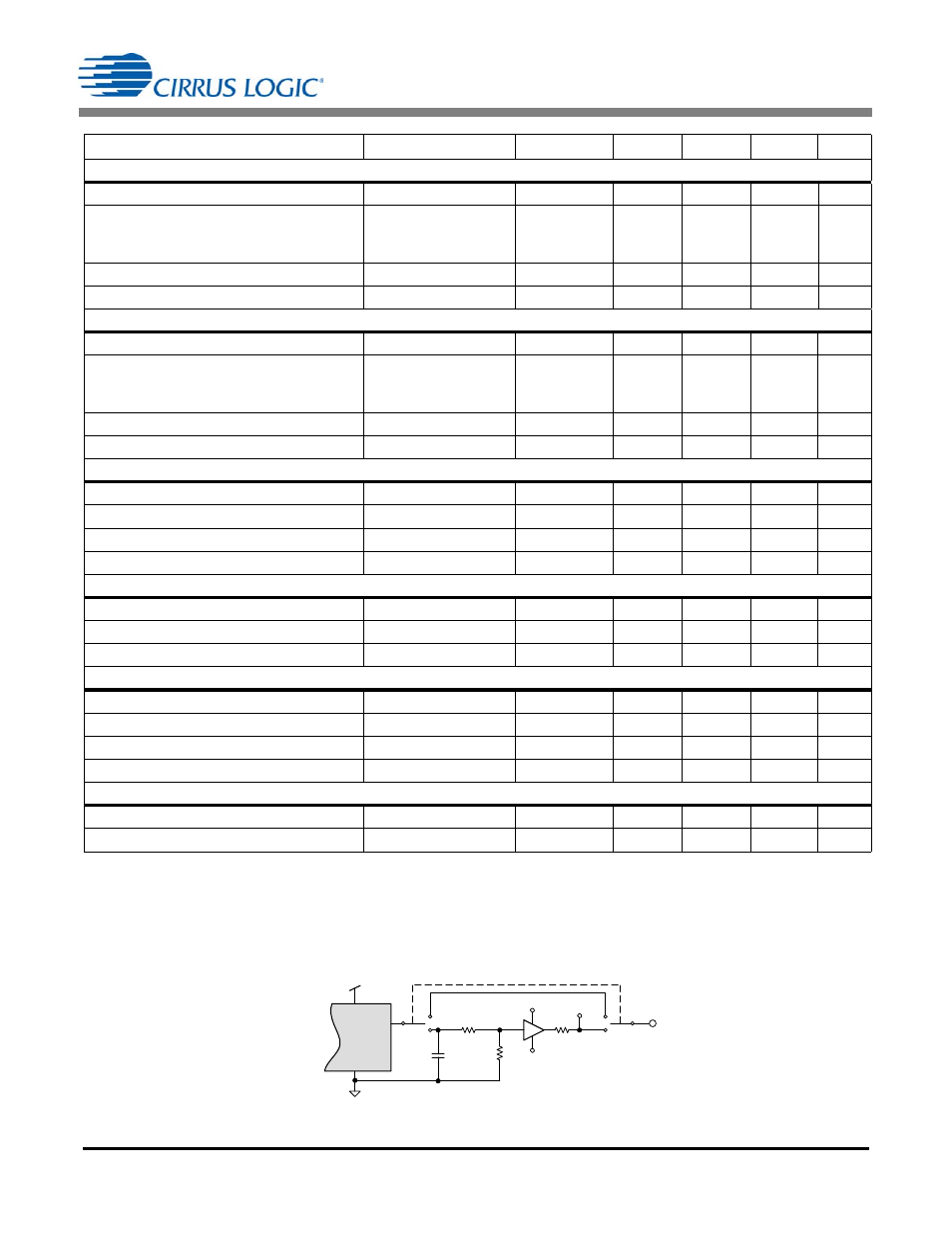
5.
For test purposes, load capacitance C
L
is 0.25nF and is connected as shown in the following diagram.
Second Stage Zero-current Detect
FBZCD Threshold
V
FBZCD(th)
-
200
-
mV
FBZCD Blanking
CS1610/12
CS1611/13
t
FBZCB
-
-
2
2.8
-
-
s
s
ZCD Sink Current
I
ZCD
-2
-
-
mA
FBAUX Upper Voltage
I
ZCD
= 1mA
-
V
DD
+0.6
-
V
Second Stage Pulse Width Modulator
Minimum On Time
-
0.55
-
s
Maximum On Time
CS1610/11/13
CS1612
-
-
8.8
12.0
-
-
s
s
Minimum Switching Frequency
t
FB(Min)
-
625
-
Hz
Maximum Switching Frequency
t
FB(Max)
-
200
-
kHz
Second Stage Gate Driver
Output Source Resistance
V
DD
= 12V
Z
OUT
-
24
-
Output Sink Resistance
V
DD
= 12V
Z
OUT
-
11
-
Rise Time
C
L
= 0.25nF
-
-
30
ns
Fall Time
C
L
= 0.25nF
-
-
20
ns
Second Stage Protection
Overcurrent Protection (OCP)
V
OCP(th)
-
1.69
-
V
Overvoltage Protection (OVP)
V
OVP(th)
-
1.25
-
V
Open Loop Protection (OLP)
V
OLP(th)
-
200
-
mV
External Overtemperature Protection (eOTP), Boost Peak Current, Second Stage Frequency Gain
Pull-up Current Source – Maximum
I
CONNECT
-
80
-
A
Conductance Accuracy
-
-
±5
Conductance Offset
-
±250
-
nS
Current Source Voltage Threshold
V
CONNECT(th)
-
1.25
-
V
Internal Overtemperature Protection (iOTP)
Thermal Shutdown Threshold
T
SD
-
135
-
ºC
Thermal Shutdown Hysteresis
T
SD(Hy)
-
14
-
ºC
Parameter
Condition
Symbol
Min
Typ
Max
Unit
GD OUT
GD
GND
VDD
Buffer
S
1
R
1
R
2
R
3
TP
+15V
-15V
S
2
V
DD
C
L
0.25nF