Introduction, Fbsense, Fbaux – Cirrus Logic CS1613 User Manual
Page 2: Bstout, Clamp, Sgnd, Source, Fbgain, Ipk eotp, Bstaux
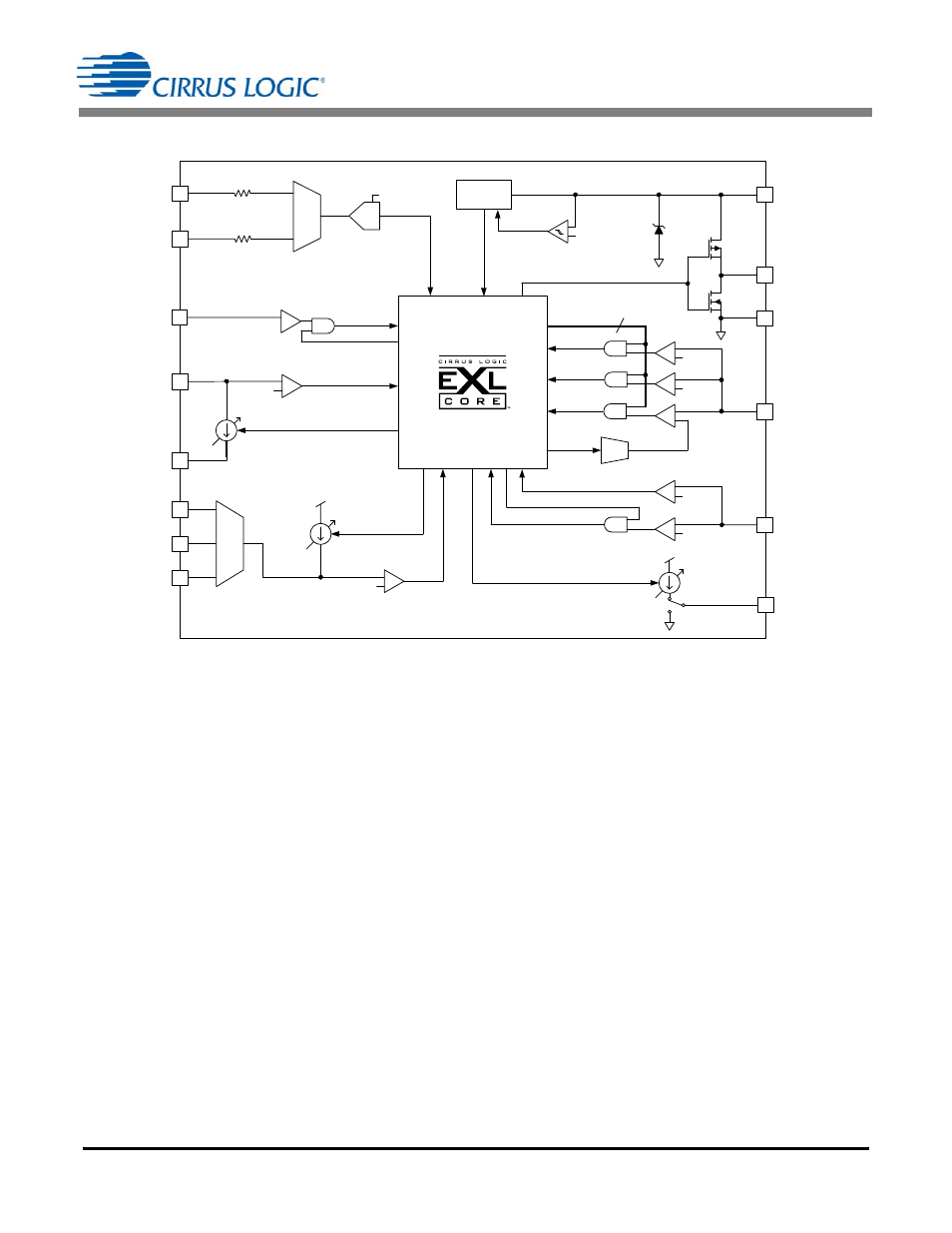
CS1610/11/12/13
2
DS929F6
1. INTRODUCTION
A typical schematic using the CS1610/11 for flyback
applications is shown on the previous page.
Startup current is provided from a patent-pending, external,
high-voltage, source-follower network. In addition to providing
startup current, this unique topology is integral in providing
compatibility with digital dimmers by ensuring V
DD
power is
always available to the IC. During steady-state operation, an
auxiliary winding on the boost inductor back-biases the
source-follower circuit and provides steady-state operating
current to the IC to improve system efficiency.
The rectified input voltage is sensed as a current into pin IAC
and is used to control the adaptive dimmer compatibility
algorithm and extract the phase of the input voltage for output
dimming control. During steady-state operation, the external
high-voltage, source-follower circuit is source-switched in
critical conduction mode (CRM) to boost the input voltage.
This allows the boost stage to maintain good power factor,
provide dimmer compatibility, reduce bulk capacitor ripple
current, and provide a regulated input voltage to the second
stage.
The output voltage of the CRM boost is sensed by the current
into the boost output voltage sense pin BSTOUT. The quasi-
resonant second stage is implemented with peak-current
mode primary-side control, which eliminates the need for
additional components to provide feedback from the
secondary and reduces system cost and complexity.
Voltage across an external user-selected resistor is sensed
through pin FBSENSE to control the peak current through the
second stage inductor. Leading-edge and trailing-edge
blanking on pin FBSENSE prevents false triggering.
Pin FBAUX is used to sense the second stage inductor
demagnetization to ensure quasi-resonant switching of the
output stage.
When an external negative temperature coefficient (NTC)
thermistor is connected to the eOTP pin, the
CS1610/11/12/13 monitors the system temperature, allowing
the controller to reduce the output current of the system. If the
temperature reaches a designated high set point, the IC is
shut down and stops switching.
V
Z
POR
+
-
Voltage
Regulator
14
VDD
11
FBSENSE
+
-
15
FBAUX
+
-
13
GD
2
IAC
DAC
+
-
Peak
Control
Second Stage ZCD
+
-
Output Open
12
GND
OLP
+
-
16
BSTOUT
MUX
OCP
Boost ZCD
3
CLAMP
V
S T(th )
V
S TP(th )
V
OCP (th )
V
FB ZCD(th)
V
OV P (th )
V
OLP (th)
V
P k_Max(th)
9
4
SGND
5
SOURCE
+
-
+
-
I
CONNE CT
V
CONNE CT(th )
V
S OURCE(th )
10
FBGAIN
8
IPK
eOTP
15k
ADC
MUX
15k
I
ref
t
FB ZCD
I
CLA MP
t
B S TZCD
I
S OURCE
+
-
1
BSTAUX
V
FB ZCD(th )
VDD
VDD
Blank
3
Figure 1. CS1610/11/12/13 Block Diagram