3 boost auxiliary winding, 4 boost overvoltage protection, 5 voltage clamp circuit – Cirrus Logic CS1613 User Manual
Page 10: 1 clamp overpower protection, 7 quasi-resonant second stage
CS1610/11/12/13
10
DS929F6
5.4.3
Boost Auxiliary Winding
The boost auxiliary winding is used for zero-current detection
(ZCD). The voltage on the auxiliary winding is sensed through
the BSTAUX pin of the IC. It is also used to deliver current
during steady-state operation, as mentioned in section 5.2
Startup Circuit
5.4.4
Boost Overvoltage Protection
The CS1610/11/12/13 supports boost overvoltage protection
(BOP) to protect the bulk capacitor C8 (see Figure 12 on
page 10). If the boost output voltage exceeds the overvoltage
protection thresholds of 249V for a 120V system, or 448V for
a 230V system, a BOP fault signal is generated. The control
logic continuously averages this BOP fault signal, and if at any
point in time the average exceeds a set event threshold, the
boost stage is disabled. The BOP fault averaging algorithm
sets the event threshold such that the boost output voltage is
never allowed to stay above the BOP threshold for more than
1.6ms.
During a boost overvoltage protection event, the second stage
is kept enabled, and its dim input is railed to full scale. This
allows the second stage to dissipate the stored energy on bulk
capacitor C8 quickly, bringing down the boost output voltage
to a safe value. A visible flash on the LED might appear,
indicating that an overvoltage event has occurred. When the
boost output voltage drops to 195V for a 120V application or
368V for a 230V application, the boost stage is enabled, and
the system returns to normal operation.
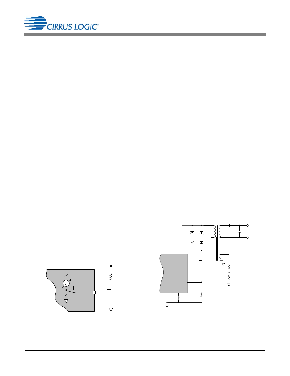
5.5 Voltage Clamp Circuit
To keep dimmers conducting and prevent them from misfiring,
a minimum power needs to be delivered from the dimmer to
the load. This power is nominally around 2W for 230V and
120 V TRIAC dimmers. At low dim angles (
90°), this excess
power cannot be converted into light by the second output
stage due to the dim mapping at light loads. Boost stage
output voltage V
BST
can rise above the safe operating voltage
of primary-side bulk capacitor C6.
The CS1610/11/12/13 provides active clamp circuitry on the
CLAMP pin, as shown in Figure 11.
A PWM control loop ensures that the boost output
voltage V
BST
does not exceed 227 V for 120VAC applications
or 424 V for 230VAC applications. This control turns on the
MOSFET of the voltage clamp circuit, allowing the clamp
circuit to sink current through the load resistor, preventing
boost output voltage V
BST
from exceeding the maximum safe
voltage.
5.5.1
Clamp Overpower Protection
The CS1610/11/12/13 clamp overpower protection (COP)
control logic averages the turn-on time of the clamp circuit. If
the output of the averaging logic exceeds 49%, a COP event
is actuated, disabling the boost and second stages. The clamp
circuitry is turned off during the fault event. The turn-on time
averaging algorithm sets the COP threshold such that the
clamp circuit cannot be continuously turned on for more than
13.8ms.
5.6 Dimming Signal Extraction and the Dim
Mapping Algorithm
When operating with a dimmer, the dimming signal is
extracted in the time domain and is proportional to the
conduction angle of the dimmer. A control variable is passed
to the quasi-resonant second stage to achieve 2% to 100%
output currents.
5.7 Quasi-resonant Second Stage
The second stage is a quasi-resonant current-regulated
DC-DC converter capable of flyback or buck operation,
delivering the highest possible efficiency at a constant current
while minimizing line frequency ripple. Primary-side control is
used to simplify system design and reduce system cost and
complexity.
The digital algorithm ensures monotonic dimming from 2% to
100% of the dimming range with a linear relationship between
the dimming signal and the LED current. The flyback stage is
controlled by sensing current in the transformer primary.
CLAMP
R10
I
CLAM P
V
BST
S1
CS1610 /11/12/ 13
VDD
3
Q3
Figure 11. CLAMP Pin Model
13
11
T1
D8
C9
LED +
LED -
D7
R12
Z2
C8
R11
R13
R
FB GA IN
Q4
FBGAIN
FBAUX
GND
GD
FBSENSE
15
9
12
CS1610/11
V
B S T
Figure 12. Flyback Model