Ic grounding practices, An346 – Cirrus Logic CS160x User Manual
Page 4
AN346
4
2.2
Placement of the CS1501 Relative to the Power Stage
– The IC should be placed away from power switching devices & traces.
– Placing the IC directly under the boost inductor is not recommended. Air-gapped cores radiate
magnetic flux which can cause noise on signal traces.
– Placing the IC immediately after the PFC output capacitors as shown in Figure 3, 4, and 5 offers a
good trade-off between power and signal integrity. This is because all the signals beyond the bulk
capacitor can be considered DC.
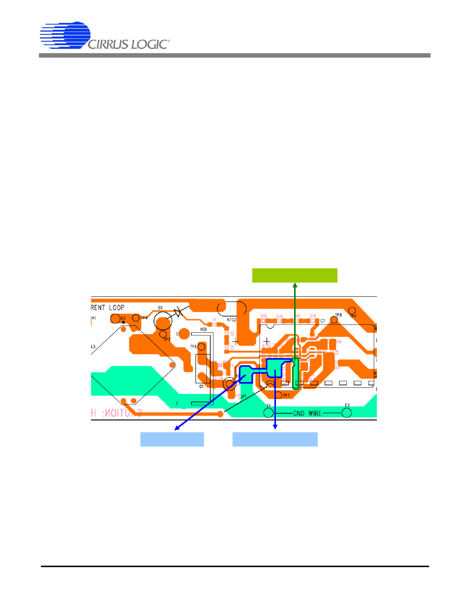
3. IC GROUNDING PRACTICES
Signal ground should be separate from the power ground. It is recommended that the sensitive IC ground
be referenced to the negative of the bulk capacitor C14 at the PFC output as shown in Figure 4.
The ground under the IC should be maximized. This ground can be divided into two sections:
– Gate drive ground, which is noisy and can carry currents up to 1A.
– Decoupling for sense lines. Figure 4 shows that these are separated.
As shown in Figure 4, the noisy current from the gate drive return enters the IC pin. The ground trace that
continues beyond the gate drive is clean and is strictly used for decoupling the sense lines. By maximizing
the signal ground around the IC and especially those pertaining to the high di/dt currents on the gate
return, the IC can have a clean reference.
Figure 4. Ground Routing Around the IC and V
DD
Path & Location of Decoupling Capacitor
Dirty Ground carrying gate
current
Clean Analog Ground for
Decoupling Sensitive Nodes
Link Capacitor
Negative