Clock divide command byte, Clock divide register, Table 6-3: clock divide bits – PNI RM3000 Sensor Suites User Manual
Page 40: 1 clock divide command byte, 2 clock divide register

PNI Sensor Corporation
Doc #1015673 r08
RM3000 & RM2000 Sensor Suite User Manual
– July 2012
Page 40 of 41
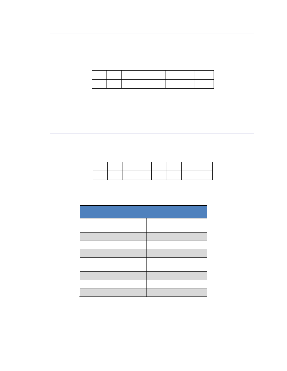
6.2.1 Clock Divide Command Byte
The Command Byte to initiate reading or writing to the Clock Divide Register is defined
as follows:
Bit #
7
6
5
4
3
2
1
0
Value
1
R/W
0
0
0
0
0
0
R/W: Read/Write
When HIGH signifies a Read operation from the Clock Divide Register. When LOW
signifies a Write operation to the Clock Divide Register.
6.2.2 Clock Divide Register
The Clock Divide Register is defined as follows:
Bit #
7
6
5
4
3
2
1
0
Value
0
0
0
0
0
CD2 CD1 CD0
Table 6-3: Clock Divide Bits
Clock Divide Value
CD2
CD1
CD0
1
(Standard Mode default)
0
0
0
2
0
0
1
4
0
1
0
8
0
1
1
16
(Legacy Mode default)
1
0
0
16
1
0
1
16
1
1
0
16
1
1
1
This manual is related to the following products:
