Figure 4. jbw 10w mechanical outline diagram, Figure 5. input/output connections – KEPCO JBW 10W Series User Manual
Page 4
4
228-1412 REV 5
061510
KEPCO, INC. 131-38 SANFORD AVENUE FLUSHING, NY. 11355 U.S.A. TEL (718) 461-7000 FAX (718) 767-1102
http://www.kepcopower.com email: [email protected]
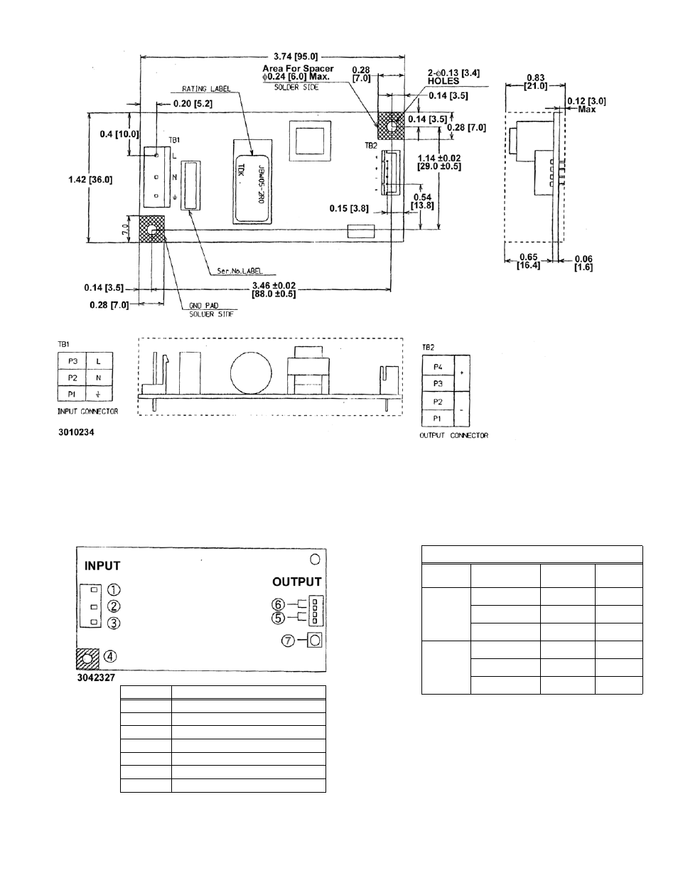
FIGURE 4. JBW 10W MECHANICAL OUTLINE DIAGRAM
FIGURE 5. INPUT/OUTPUT CONNECTIONS
NOTES:
1.
Dimensions are in inches, dimensions in brackets are in millimeters.
2.
TOLERANCES: ±0.04” [±1.0 mm] unless specified.
3. WEIGHT: 1.76 oz. (50 gr.) max.
4. PCB: Thickness = 0.06 ± 0.008 in. (1.6 ± 0.2mm)
Mating Connectors(4)
Connector
Terminal Pin
Socket
Housing
MFR
Input
SVH-21T-P1.1
VHR-5N
JST(1)
T101
H101-05
LCE(2)
50539-8100
51144-0500
MLX(3)
Output
SXH-001T-P0.6 XHP-4
JST(1)
T221-01
H221-04
LCE(2)
67262-001
67261-0400
MLX(3)
(1) JST= Japan Solderless Terminal Mfg. Co.
(2) LCE= Long Chu Electronics Co.
(3) MLX = Molex
(4) Optional cable kit (P/N 219-0406) includes
one input and one output cable (one meter
long) with mating connectors for TB1 and
TB2, unterminated at other end.
Terminal
Function
1
Input L
2
Input N
3
Ground
4
Ground Pad
5
Output (-)
6
Output (+)
7
Output ADJ (JBW 03-2R0 only
- ABC-DM SERIES (96 pages)
- ATE (all models) QUICK START GUIDE (8 pages)
- SN 488-D (94 pages)
- SN 488-D (14 pages)
- SN 488-D (16 pages)
- BHK-MG 200W (Full Rack) Series (152 pages)
- BHK-MG 40W (Half Rack) Series (148 pages)
- BIT 232 (72 pages)
- BIT 4882 (56 pages)
- BIT 4886 Quick Start Guide (4 pages)
- BIT 4886 Operator Manual (92 pages)
- BOP 100W, 200W, 400W (M, D) Quick Start Guide (8 pages)
- BOP 20-5ML Modification Sheet (1 page)
- BOP 20-10MC Modification Sheet (2 pages)
- BOP 36-6MC Modification Sheet (2 pages)
- BOP 100-2MC Modification Sheet (2 pages)
- BOP 50-4MC Modification Sheet (2 pages)
- BOP 100-2ML Modification Sheet (2 pages)
- BOP 72-3ML Modification Sheet (2 pages)
- BOP 50-4ML Modification Sheet (2 pages)
- BOP 36-6ML Modification Sheet (2 pages)
- BOP 20-10ML Modification Sheet (2 pages)
- BOP 72-6MC Modification Sheet (2 pages)
- BOP 36-12MC Modification Sheet (2 pages)
- BOP 20-20MC Modification Sheet (2 pages)
- BOP 100-4ML Modification Sheet (2 pages)
- BOP 72-6ML Modification Sheet (2 pages)
- BOP 50-8ML Modification Sheet (2 pages)
- BOP 36-12ML Modification Sheet (2 pages)
- BOP 20-20ML Modification Sheet (2 pages)
- BOP 1KW-MG Quick Start Guide (16 pages)
- BOP 1KW-MG Quick Reference Guide (2 pages)
- BOP 1KW-MG Operator Manual, Firmware Ver.4.12 and higher (196 pages)
- BOP 1KW-MG Operator Manual, Firmware Ver.4.08 to 4.11 (194 pages)
- BOP 1KW-MG Operator Manual, Firmware Ver.3.05 to 4.07 (194 pages)
- BOP 1KW-MG Operator Manual, Firmware Ver.2.48 to 3.04 (188 pages)
- BOP 1KW-MG Operator Manual, Firmware Ver.2.38 to 2.47 (188 pages)
- BOP 1KW-MG Operator Manual, Firmware Ver.2.01 to 2.37 (176 pages)
- BOP 1KW as Solar Device Tester Quick Start Guide (3 pages)
- BOP-GL 1KW Quick Start Guide (16 pages)
- BOP-GL 1KW Operator Manual Firmware Ver.3.05 and higher (168 pages)
- BOP-HV (48 pages)
- CA 26 (2 pages)
- CA 27 (2 pages)
- CA 29 (2 pages)