Pam8610, Pin descriptions – Diodes PAM8610 User Manual
Page 2
PAM8610
Document number: DSxxxxx Rev. 1 - 2
2 of 15
June 2013
© Diodes Incorporated
PAM8610
A Product Line of
Diodes Incorporated
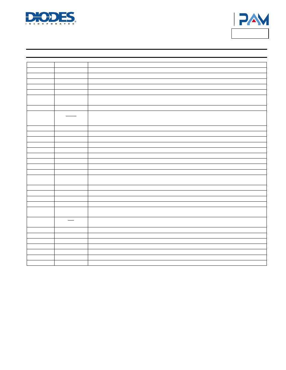
Pin Descriptions
Pin Number
Pin Name
Function
1
RINN
Negative differential audio input for right channel.
2 RINP
Positive
differential audio input for right channel.
3
AVDD
5V Analog VDD
4
VREF
Analog reference for gain control section.
5
VOLUME
DC voltage that sets the gain of the amplifier.
6 REF
GND
Ground for gain control circuitry. Connect to AGND. If using a DAC to control the
volume, connect the DAC ground to this terminal.
7 AGND1
Analog
GND
8
FADE
Input for controlling volume ramp rate when cycling SD or during power-up. A
logic low on this pin places the amplifier in fade mode. A logic high on this pin
allows a quick transition to the desired volume setting.
9
LINP
Positive differential audio input for left channel.
10
LINN
Negative differential audio input for left channel.
11, 20
PGNDL
Power ground for left channel H-bridge.
12, 19
PVCCL
Power supply for left channel H-bridge, not connected to PVCCR or AVCC.
13, 14
LOUTN
Class-D 1/2-H-bridge negative output for left channel.
15
BSLN
Bootstrap I/O for left channel, negative high-side FET.
16
BSLP
Bootstrap I/O for left channel, positive high-side FET.
17, 18
LO UTP
Class-D 1/2-H-bridge positive output for left channel.
21
VCLAMPL
Internally generated voltage supply for left channel bootstrap capacitors.
22 CO
SC
I/O for charge/discharging currents onto capacitor for ramp generator triangle
wave biased at V2P5.
23
RO SC
Current setting resistor for ramp generator. Nominally equal to 1/8*VCC.
24, 28
AGND
Analog GND
25
MUTE
A logic high on this pin disables the outputs and a logic low enables the outputs.
26
AVCC
High-voltage analog power supply (7V to 15V)
27 V2P5
2.5V Reference for analog cells, as well as reference for unused audio input
when using single-ended inputs.
29
SD
Shutdown signal for IC (low = shutdown, high = operational). TTL logic levels with
compliance to VCC.
30
VCLAMPR
Internally generated voltage supply for right channel bootstrap capacitors.
31, 40
PGNDR
Power ground for right channel H-bridge.
32, 39
PVCCR
Power supply for right channel H-bridge, not connected to PVCCL or AVCC.
33, 34
ROUTP
Class-D 1/2-H-bridge positive output for right channel.
35
BSRP
Bootstrap I/O for right channel, positive high-side FET.
36
BSRN
Bootstrap I/O for right channel, negative high-side FET.
37, 38
ROUTN
Class-D 1/2-H-bridge negative output for right channel.