Pam8610, Application information – Diodes PAM8610 User Manual
Page 10
PAM8610
Document number: DSxxxxx Rev. 1 - 2
10 of 15
June 2013
© Diodes Incorporated
PAM8610
A Product Line of
Diodes Incorporated
Application Information
(cont.)
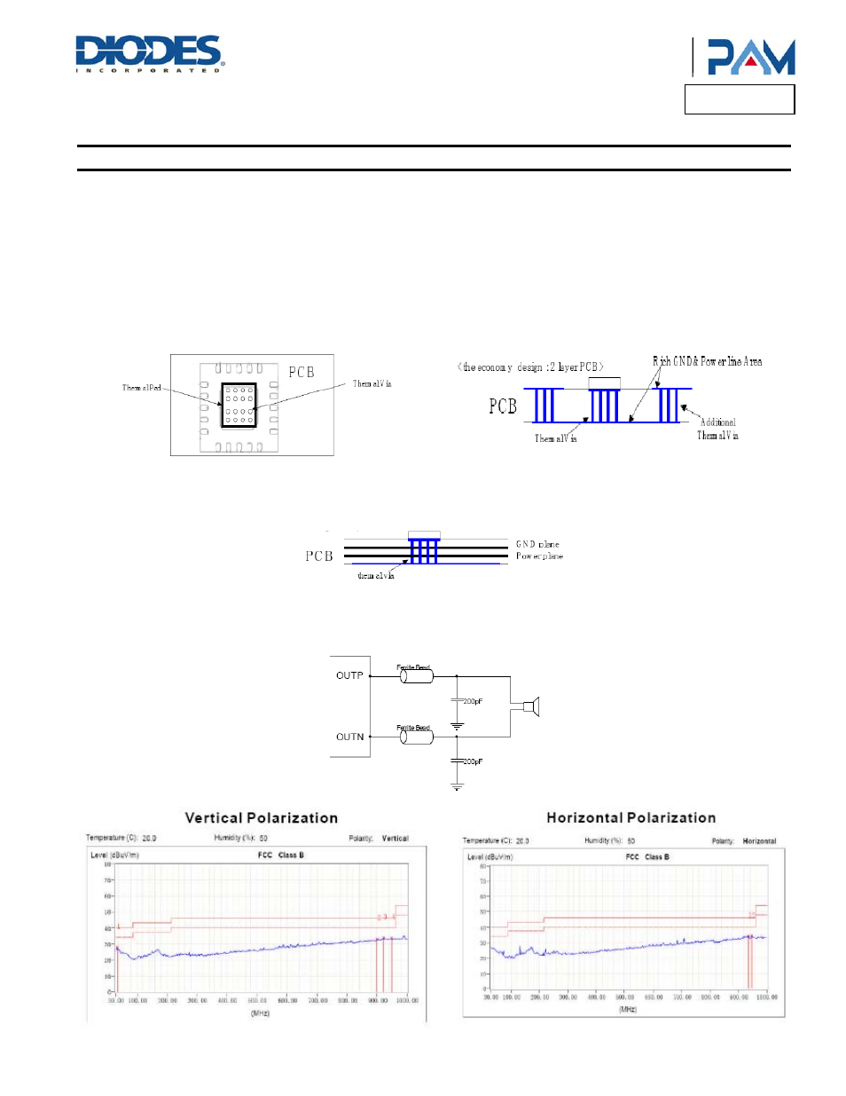
Heat Dissipation in PCB Design
Generally, class-D amplifiers are high efficiency and need no heat sink. For high power ones that has high dissipation power, the heat sink may
also not necessary if the PCB is carefully designed to achieve good heat by the PCB itself.
Dual-Side PCB
To achieve good heat, the PCB’s copper plate should be thicker than 0.035mm and both sides of the PCB should be utilized for heat sink.
The thermal pad on the bottom of the device should be soldered to the plate of the PCB, and via holes, usually 9 to 16, should be drilled in the
PCB area under the device and deposited copper on the vias should be thick enough so that the heat can be dissipated to the other side of the
plate. There should be no insulation mask on the other side of the copper plate. It is better to drill more vias around the device if possible.
4-Layer PCB
If it is 4-layer PCB, the two middle layers of grounding and power can be employed for heat dissipation, isolating them into serval islands to avoid
short between ground and power.
Consideration for EMI
Filters are not required if the traces from the amplifier to the speakers are short (<20cm). But most applications require a ferrite bead filter as
shown in below figure. The ferrite bead filter reduces EMI of around 1MHz and higher to meet the FCC and CE's requirements. It is
recommended to use a ferrite bead with very low impedances at low f requenc ies and high impedance at high frequencies (above 1MHz).
The EMI characteristics are as follows after employing the ferrite bead.