Pam8320 new product, Pin descriptions, Functional block diagram – Diodes PAM8320 User Manual
Page 2
PAM8320
Document number: DS36610 Rev. 1 - 2
2 of 11
October 2013
© Diodes Incorporated
PAM8320
New Product
A PRODUCT LINE OF
DIODES INCORPORATED
Pin Descriptions
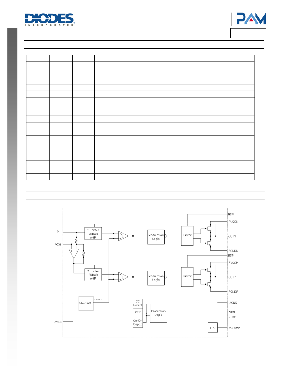
Pin Name I/O/P
Description
1
PVCCN
P
Power supply for negative H-bridge, not connected to PVCCP or AVCC
2 SDN I
Shutdown signal for IC (low=shutdown, high=operational). TTL logic levels with compliance to
AVCC
3
IN
I
Audio input
4
VCM
O
Reference for analog cells
5,6
AGND
P
Analog ground for digital/analog cells in core
7 VCLAMP P
Internally generated voltage supply for bootstrap. Not to be used as a supply or connected to
any component other than the decoupling capacitor.
8
PVCCP
P
Power supply for positive H-bridge, not connected to PVCCN or AVCC
9
PGNDP
P
Power ground for positive H-bridge
10
OUTP
O
Positive BTL output
11
BSP
I/O
Bootstrap terminal for high-side drive of positive BTL output
12 MUTE I
A logic high on this pin disables the outputs. A low on this pin enables the outputs. TTL logic
levels with compliance to AVCC
13
AVCC
P
High-voltage analog power supply
14
BSN
I/O
Bootstrap terminal for high-side drive of negative BTL output
15
OUTN
O
Negative BTL output
16
PGNDN
P
Power ground for negative H-bridge
Functional Block Diagram