Pam8301, Pin descriptions, Functional block diagram – Diodes PAM8301 User Manual
Page 2: Absolute maximum ratings, Recommended operating conditions
PAM8301
Document number: DSxxxxx Rev. 1 - 3
2 of 10
July 2013
© Diodes Incorporated
PAM8301
A Product Line of
Diodes Incorporated
Pin Descriptions
Pin
Number
Pin
Name
Function
1 OUT-
Negative Output
2 GND
Ground
3 IN
Input
4 SD
Shutdown, Active Low
5 VDD
Power Supply
6 OUT+
Positive Output
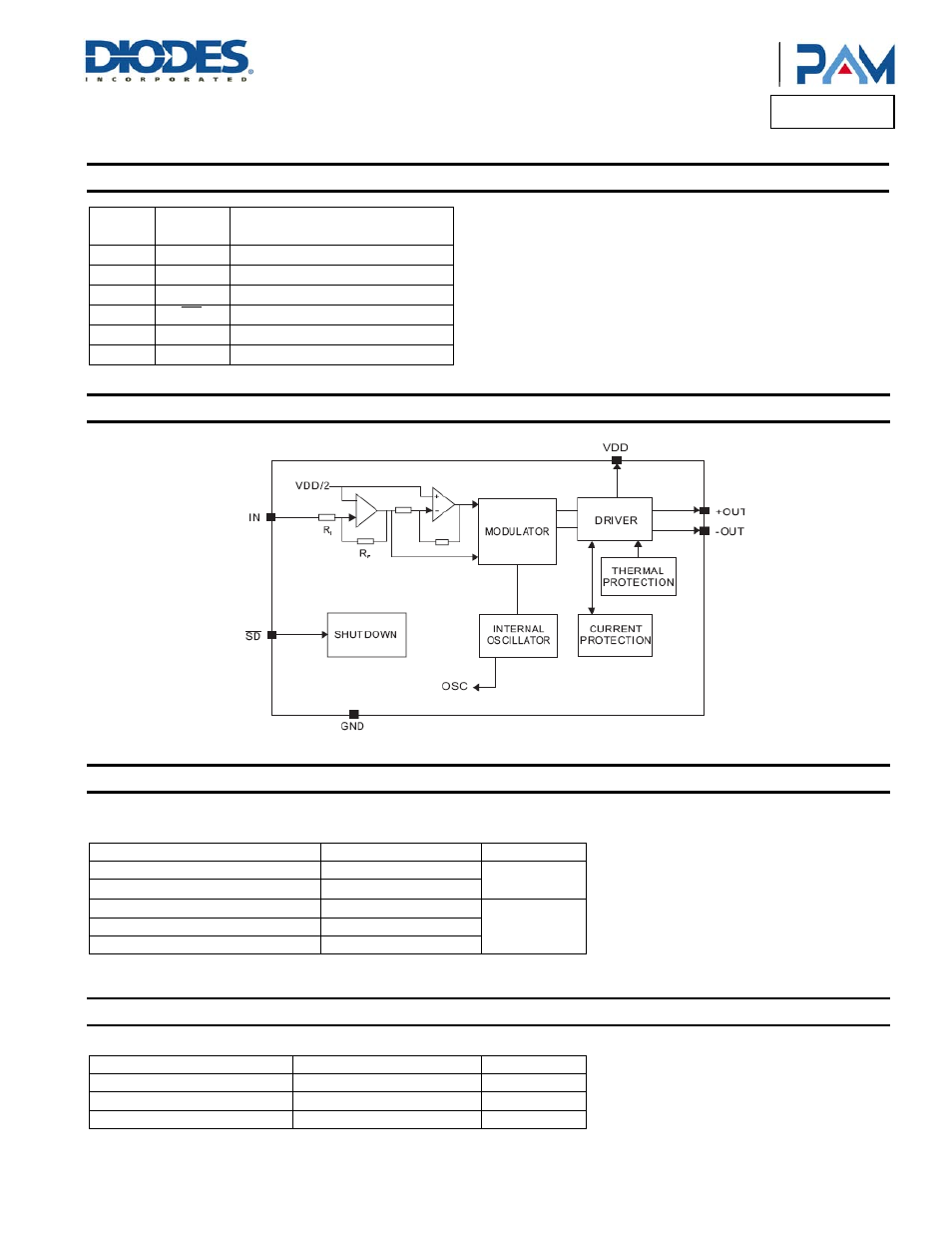
Functional Block Diagram
Absolute Maximum Ratings
(@T
A
= +25°C, unless otherwise specified.)
These are stress ratings only and functional operation is not implied. Exposure to absolute maximum ratings for prolonged time periods may
affect device reliability. All voltages are with respect to ground.
Parameter Rating
Unit
Supply Voltage at No Input Signal
6.0
V
Input Voltage Range
-0.3 to V
DD
+0.3
Maximum Junction Temperature
150
°C
Storage Temperature
-65 to +150
Soldering Temperature
300, 5sec
Recommended Operating Conditions
(@T
A
= +25°C, unless otherwise specified.)
Parameter Rating
Unit
Supply Voltage Range
2.5 to 5.5
V
Operation Temperature Range
-40 to +85
°C
Junction Temperature Range
-40 to +125
°C