Pam8012, Application information – Diodes PAM8012 User Manual
Page 9
PAM8012
Document number: DSxxxxx Rev. 1 - 3
9 of 14
www.diodes.com
October 2012
© Diodes Incorporated
PAM8012
A Product Line of
Diodes Incorporated
Application Information
(cont.)
Over Temperature Protection (OTP)
Thermal protection on the PAM8012 prevents the device from damage when the internal die temperature exceeds +150°C. There is a +15°C
tolerance on this trip point from device to device. Once the die temperature exceeds the set point, the device will enter the shutdown state and
the outputs are disabled. This is not a latched fault. The thermal fault is cleared once the temperature of the die decreased by +40°C. This large
hysteresis will prevent motor boating sound well and the device begins normal operation at this point with no external system interaction.
POP and Click Circuitry
The PAM8012 contains circuitry to minimize turnon and turn-off transients or “click and pops”, where turn-on refers to either power supply turn-
on or device recover from shutdown mode. When the device is turned on, the amplifiers are internally muted. An internal current source ramps
up the reference voltage. The device will remain in mute mode until the reference voltage reach half supply voltage, ½ V
DD
. As soon as the
reference voltage is stable the device will begin full operation. For the best power-off pop performance, the amplifier should be set in shutdown
mode prior to removing the power supply voltage.
PCB Layout Guidelines
Grounding
It is recommended to use plane grounding. Noise currents in the output power stage need to be returned to output noise ground and nowhere
else. When these currents circulate elsewhere, they may get into the power supply, or the signal ground, etc, even worse, they may form a loop
and radiate noise. Any of these instances results in degraded amplifier performance. The output noise ground that the logical returns for the
output noise currents with Class-D switching must tie to system ground at the power exclusively. Signal currents for the inputs, reference need
to be returned to quite ground. This ground only ties to the signal components and the GND pin. GND then ties to system ground.
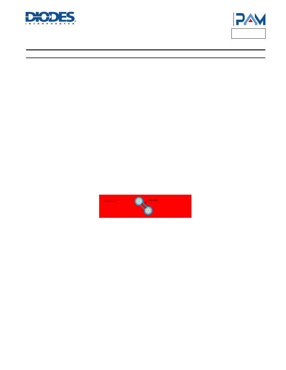
Power Supply Line
It is recommended that all the trace could be routed as short and thick as possible. For the power line layout, just imagine water stream, any
barricade placed in the trace (shown in Figure 2) could result in the bad performance of the amplifier.
Figure 2: Power Line
Components Placement
Decoupling capacitors as previously described, the high-frequency 1µF decoupling capacitors should be placed as close to the power supply
terminals V
DD
as possible. Large bulk power supply decoupling capacitors (10µF or greater) should be placed near the PAM8012 on the V
DD
terminal.
Input resistors and capacitors need to be placed very close to input pins.
Output filter - The ferrite EMI filter should be placed as close to the output terminals as possible for the best EMI performance, and the
capacitors used in the filters should be grounded to system ground.