Pam2327, Pin descriptions, Functional block diagram – Diodes PAM2327 User Manual
Page 2: Absolute maximum ratings
PAM2327
Document number: DS36277 Rev. 2 - 2
2 of 11
July 2013
© Diodes Incorporated
PAM2327
A Product Line of
Diodes Incorporated
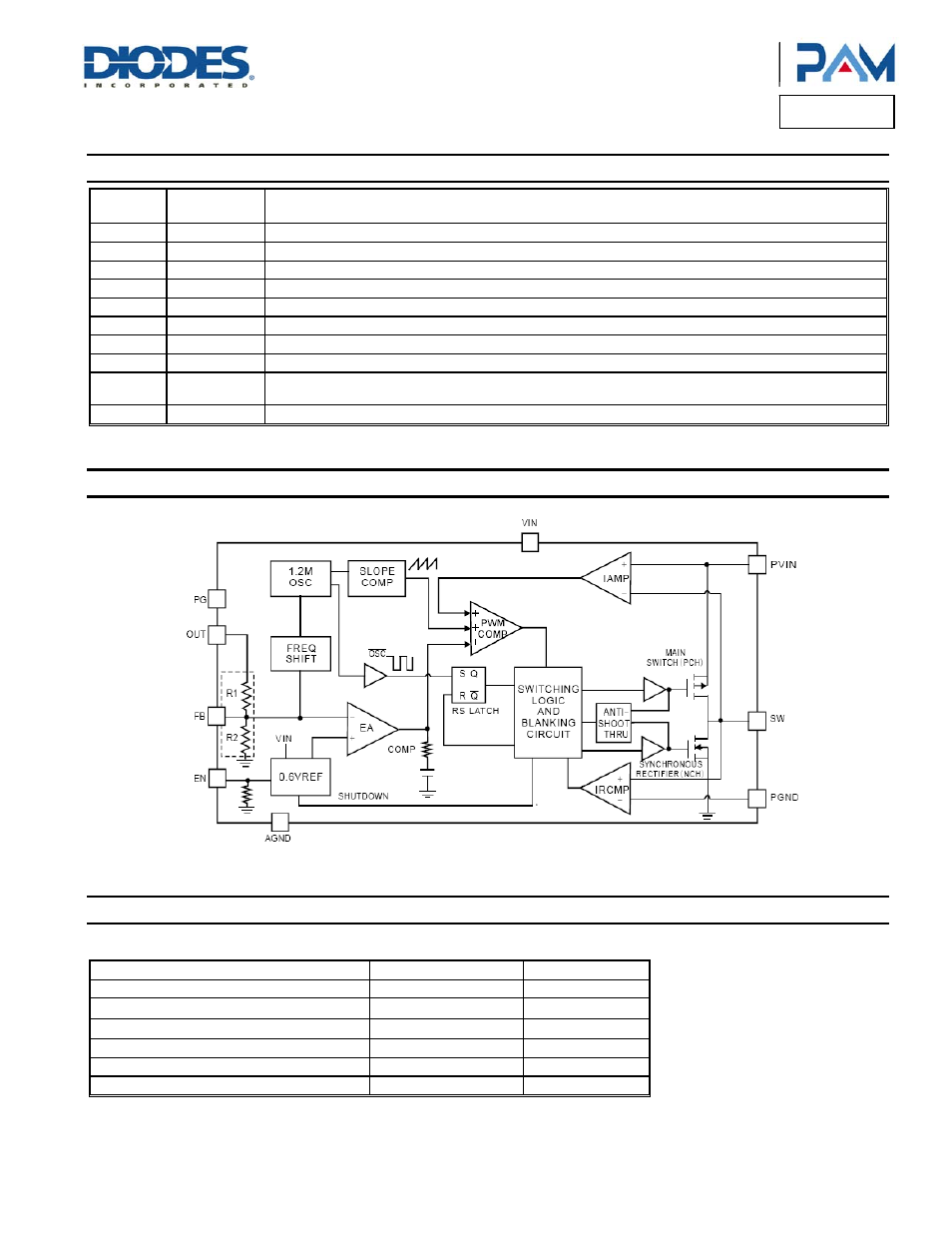
Pin Descriptions
Pin
Number
Pin
Name
Function
1
PVIN
Supply Voltage to power FETs. PVIN is connected to VIN internally.
2, 11
SW
Switch Output. Pin 2 and 11 can be connected together.
3, 12
PGND
Power Ground. Pin 3 and 12 can be connected together.
4
AGND
Quiet ground for controller circuits
5
NC
Leave this pin open. Do not connect it to ground.
6
OUT
Input sense pin for output voltage
7
FB
Feedback. An external resistor divider from the output to GND, tapped to the FB pin, sets the output voltage.
8 EN
On/Off
Control.
9 PG
Power Good Indicator. The output of this pin is an open drain with internal pull up resistor to VIN. PG is pulled
up to VIN when the FB voltage is within 10% of the regulation level, otherwise it is LOW.
10
VIN
Supply Voltage to internal control circuitry. VIN is connected to PVIN internally.
Functional Block Diagram
Absolute Maximum Ratings
(@T
A
= +25°C, unless otherwise specified.)
These are stress ratings only and functional operation is not implied. Exposure to absolute maximum ratings for prolonged time periods may
affect device reliability. All voltages are with respect to ground.
Parameter Rating
Unit
Input Voltage
-0.3 to +6.5
V
EN, FB Pin Voltage
-0.3 to V
IN
V
SW Pin Voltage
-0.3 to (V
IN
+0.3)
V
Junction Temperature
150
°C
Storage Temperature Range
-65 to +150
°C
Soldering Temperature
300, 5sec
°C