Absolute maximum ratings thermal resistance – Diodes ZXTP19100CG User Manual
Page 2
ZXTP19100CG
Issue 1- February 2008
2
www.zetex.com
© Zetex Semiconductors plc 2008
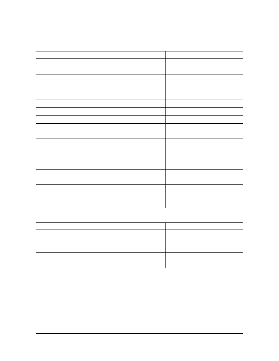
Absolute maximum ratings
Thermal resistance
NOTES:
(a) For a device surface mounted on 15mm x 15mm x 0.6mm FR4 PCB with high coverage of single sided 1oz copper, in
still air conditions.
(b) Mounted on 25mm x 25mm x 0.6mm FR4 PCB with high coverage of single sided 1oz copper, in still air conditions.
(c) Mounted on 50mm x 50mm x 0.6mm FR4 PCB with high coverage of single sided 2oz copper, in still air conditions.
(d) As (c) above measured at t<5 seconds.
(e) Junction to case (collector tab). Typical
Parameter
Symbol
Limit
Unit
Collector-Base voltage
V
CBO
-110
V
Collector-Emitter voltage (forward blocking)
V
CEX
-110
V
Collector-Emitter voltage
V
CEO
-100
V
Emitter-Collector voltage (reverse blocking)
V
ECO
-7
V
Emitter-Base voltage
V
EBO
-7
V
Continuous Collector current
(c)
I
C
-2
A
Base current
I
B
-1
A
Peak pulse current
I
CM
-3
A
Power dissipation at T
A
=25
°
C
(a)
Linear derating factor
P
D
1.2
9.6
W
mW/
°
C
Power dissipation at T
A
=25
°
C
(b)
Linear derating factor
P
D
1.6
12.8
W
mW/
°
C
Power dissipation at T
A
=25
°
C
(c)
Linear derating factor
P
D
3.0
24
W
mW/
°
C
Power dissipation at T
A
=25
°
C
(d)
Linear derating factor
P
D
5.3
42
W
mW/
°
C
Power dissipation at T
C
=25
°
C
(e)
Linear derating factor
P
D
10.2
81
W
mW/
°
C
Operating and storage temperature range
T
j
, T
stg
-55 to 150
°
C
Parameter
Symbol
Limit
Unit
Junction to ambient
(a)
R
⍜
JA
104
°
C/W
Junction to ambient
(b)
R
⍜
JA
78
°
C/W
Junction to ambient
(c)
R
⍜
JA
42
°
C/W
Junction to ambient
(d)
R
⍜
JA
23.5
°
C/W
Junction to case
(e)
R
⍜
JC
12.3
°
C/W