Maximum ratings, Thermal characteristics – Diodes MMDTA06 User Manual
Page 2
MMDTA06
Document Number: DS35114 Rev: 1 - 2
2 of 8
April 2011
© Diodes Incorporated
MMDTA06
ADVAN
CE I
N
F
O
RM
ATI
O
N
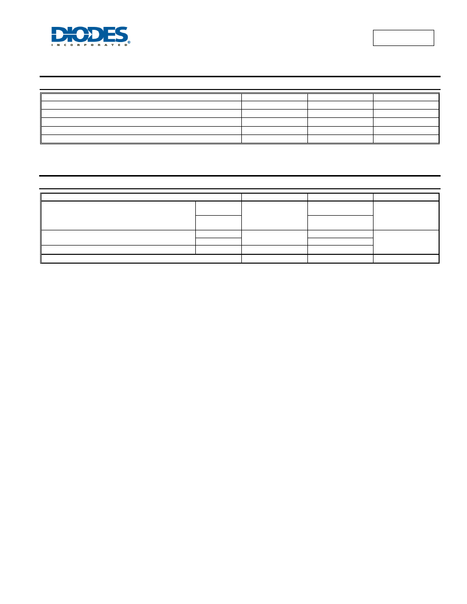
Maximum Ratings
@T
A
= 25°C unless otherwise specified
Characteristic Symbol
Value
Unit
Collector-Base Voltage
V
CBO
80 V
Collector-Emitter Voltage
V
CEO
80 V
Emitter-Base Voltage
V
EBO
4 V
Continuous Collector Current
I
C
500 mA
Peak Pulse Collector Current
I
CM
1 A
Thermal Characteristics
@T
A
= 25°C unless otherwise specified
Characteristic Symbol
Value
Unit
Power Dissipation
Linear Derating Factor
(Notes 5 & 6)
P
D
1.28
10.3
W
mW/
°C
(Notes 4 & 6)
0.90
7.14
Thermal Resistance, Junction to Ambient
(Notes 5 & 6)
R
θJA
97
°C/W
(Notes 4 & 6)
140
Thermal Resistance, Junction to Lead
(Note 7)
R
θJL
103
Operating and Storage Temperature Range
T
J
, T
STG
-55 to +150
°C
Notes:
4. For a device surface mounted on 25mm x 25mm x 1.6mm FR4 PCB with high coverage of single sided 1oz copper, in still air conditions; the device is
measured when operating in a steady-state condition.
5. Same as note (4), except the device is measured at t
≤ 5 sec.
6. For a dual device with one active die.
7. Thermal resistance from junction to solder-point (at the end of the collector lead).