Maximum ratings, drdp006w pnp transistor, Maximum ratings, switching diode – Diodes DRD (xxxx) W User Manual
Page 2

DS30573 Rev. 10 - 2
2 of 9
www.diodes.com
DRD (xxxx) W
© Diodes Incorporated
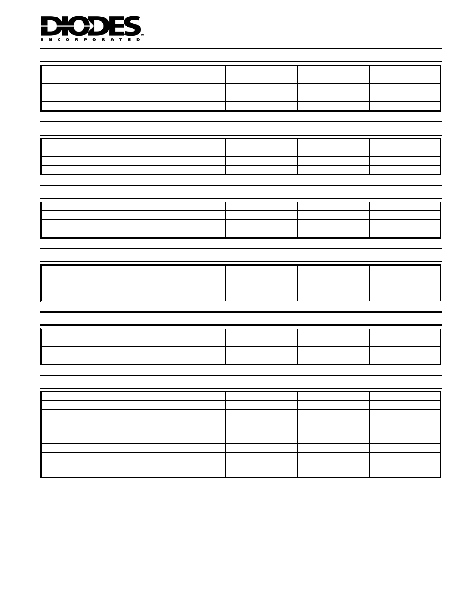
Maximum Ratings, DRDP006W PNP Transistor
@T
A
= 25°C unless otherwise specified
Characteristic
Symbol
Value
Unit
Collector-Base Voltage
V
CBO
-60
V
Collector-Emitter Voltage
V
CEO
-60
V
Emitter-Base Voltage
V
EBO
-5.0
V
Collector Current (Note 3)
I
C
-600
mA
Maximum Ratings, DRDNB16W Pre-Biased NPN Transistor
@T
A
= 25°C unless otherwise specified
Characteristic
Symbol
Value
Unit
Supply Voltage
V
CC
50
V
Input Voltage
V
IN
-5 to +10
V
Output Current
I
C
600
mA
Maximum Ratings, DRDNB26W Pre-Biased NPN Transistor
@T
A
= 25°C unless otherwise specified
Characteristic
Symbol
Value
Unit
Supply Voltage
V
CC
50
V
Input Voltage
V
IN
-5 to +5
V
Output Current
I
C
600
mA
Maximum Ratings, DRDPB16W Pre-Biased PNP Transistor
@T
A
= 25°C unless otherwise specified
Characteristic
Symbol
Value
Unit
Supply Voltage
V
CC
-50
V
Input Voltage
V
IN
+5 to -10
V
Output Current
I
C
600
mA
Maximum Ratings, DRDPB26W Pre-Biased PNP Transistor
@T
A
= 25°C unless otherwise specified
Characteristic
Symbol
Value
Unit
Supply Voltage
V
CC
-50
V
Input Voltage
V
IN
+5 to -5
V
Output Current
I
C
-600
mA
Maximum Ratings, Switching Diode
@T
A
= 25°C unless otherwise specified
Characteristic
Symbol
Value
Unit
Non-Repetitive Peak Reverse Voltage
V
RM
100
V
Peak Repetitive Reverse Voltage
Working Peak Reverse Voltage
DC Blocking Voltage
V
RRM
V
RWM
V
R
75
V
RMS Reverse Voltage
V
R(RMS)
53
V
Forward Continuous Current (Note 3)
I
FM
500
mA
Average Rectified Output Current (Note 3)
I
O
250
mA
Non-Repetitive Peak Forward Surge Current
@ t = 1.0
μs
@ t = 1.0s
I
FSM
4.0
2.0
A
