Maximum ratings, Thermal characteristics, Electrical characteristics – Diodes DESDALC5LP User Manual
Page 2
DESDALC5LP
Document number: DS36761 Rev. 2 - 2
2 of 6
May 2014
© Diodes Incorporated
DESDALC5LP
ADVAN
CE I
N
F
O
RM
ATI
O
N
ADVANCED INFORMATION
Maximum Ratings
(@T
A
= +25°C, unless otherwise specified.)
Characteristic Symbol
Value
Unit
Conditions
Peak Pulse Power Dissipation
P
PP
150 W
8/20µs
Peak Pulse Current
I
PP
9 A
8/20µs
ESD Protection – Contact Discharge
V
ESD_Contact
±30
kV
IEC 61000-4-2 Standard
ESD Protection – Air Discharge
V
ESD_Air
±30
kV
IEC 61000-4-2 Standard
Thermal Characteristics
Characteristic Symbol
Value
Unit
Package Power Dissipation (Note 5)
P
D
250 mW
Thermal Resistance, Junction to Ambient (Note 5)
R
θJA
500
°C/W
Operating and Storage Temperature Range
T
J
, T
STG
-65 to +150
°C
Electrical Characteristics
(@T
A
= +25°C unless otherwise specified)
Characteristic
Symbol
Min
Typ
Max
Unit
Test Conditions
Reverse Breakdown Voltage
V
BR
11 13 17
V
I
R
= 1mA, pin1 to pin2
5.8 8 11
I
R
= 1mA, pin2 to pin1
Reverse Current (Note 6)
I
R
— — 25 nA
V
R
= 5V
Dynamic Resistance, from Pin 1 to Pin 2
R
DYN
— 0.19 — Ω
I
TLP
= 1A to 20A, t
P
= 100ns
Dynamic Resistance, from Pin 2 to Pin 1
R
DYN
— 0.19 — Ω
I
TLP
= 1A to 20A, t
P
= 100ns
Capacitance
C
T
— 26 30 pF
V
R
= 0V, f = 1MHz
Clamping Voltage, from Pin 1 to Pin 2
V
CL
— 21 — V
8kV contact discharge after 30ns
IEC61000-4-2
Clamping Voltage, from Pin 2 to Pin 1
V
CL
— 12 — V
8kV contact discharge after 30ns
IEC61000-4-2
Notes:
5. Device mounted on FR-4 PCB pad layout (2oz copper) as shown on Diodes, Inc. suggested pad layout AP02001, which can be found on our website at
6. Short duration pulse test used to minimize self-heating effect.
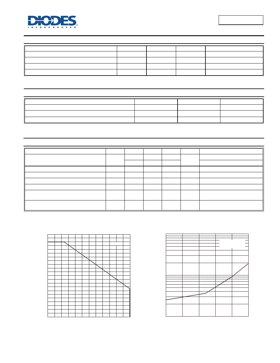
0.2
0.3
0.4
0.5
0.6
0.7
0.8
0.9
1.0
0
25
50
75
100
125
0.0
0.1
150
1.1
T (°C)
J
Figure 1 Normalized Peak Pulse Power vs.
Initial Junction Temperature
P
(
T
In
iti
al
)/
=
+
25
)
PK
J
P
(
T
In
itia
l
°C
PK
J
8/20µs
T (°C)
J
Figure 2 Leakage Current vs. Junction Temperature
(Typical Values)
I (
n
A
)
R
1
10
100
25
50
75
100
125
150
V = V
= 5V
From Pin 1 to Pin 2
R
RM