Electrical characteristics p-channel q1, Dmc4047lsd – Diodes DMC4047LSD User Manual
Page 3
DMC4047LSD
Document number: DS36206 Rev. 4 - 2
3 of 9
November 2013
© Diodes Incorporated
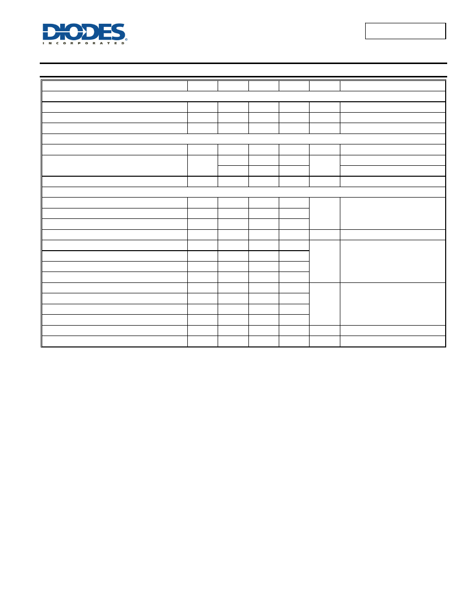
DMC4047LSD
Electrical Characteristics P-Channel Q1
(@T
A
= +25°C, unless otherwise specified.)
Characteristic Symbol
Min
Typ
Max
Unit
Test
Condition
OFF CHARACTERISTICS (Note 8)
Drain-Source Breakdown Voltage
BV
DSS
-40
V
V
GS
= 0V, I
D
= -250µA
Zero Gate Voltage Drain Current
I
DSS
-1 µA
V
DS
= -40V, V
GS
= 0V
Gate-Source Leakage
I
GSS
100 nA
V
GS
= ±20V, V
DS
= 0V
ON CHARACTERISTICS (Note 8)
Gate Threshold Voltage
V
GS(th)
-1.0
-2.2 V
V
DS
= V
GS
, I
D
= -250µA
Static Drain-Source On-Resistance
R
DS(ON)
33 45
mΩ
V
GS
= -10V, I
D
= -5A
40 55
V
GS
= -4.5V, I
D
= -4A
Diode Forward Voltage
V
SD
-0.7 -1.0 V
V
GS
= 0V, I
S
= -1.0A
DYNAMIC CHARACTERISTICS (Note 9)
Input Capacitance
C
iss
1154
pF
V
DS
= -20V, V
GS
= 0V
f = 1.0MHz
Output Capacitance
C
oss
84
Reverse Transfer Capacitance
C
rss
66
Gate Resistance
R
G
12.6
Ω
V
DS
= 0V, V
GS
= 0V, f = 1.0MHz
Total Gate Charge (V
GS
= -4.5V)
Q
g
10.6
nC
V
DS
= -20V, I
D
= -4.9A
Total Gate Charge (V
GS
= -10V)
Q
g
21.5
Gate-Source Charge
Q
gs
2.2
Gate-Drain Charge
Q
gd
3.3
Turn-On Delay Time
t
D(on)
8.7
nS
V
DS
= -20V, I
D
= -3.9A
V
GS
= -4.5V, R
G
= 1Ω
Turn-On Rise Time
t
r
19.6
Turn-Off Delay Time
t
D(off)
34.9
Turn-Off Fall Time
t
f
25.5
Body Diode Reverse Recovery Time
t
rr
9.61
nS
I
S
= -3.9A, dI/dt = 100A/μs
Body Diode Reverse Recovery Charge
Q
rr
3.30
nC
I
S
= -3.9A, dI/dt = 100A/μs
Notes:
5. Device mounted on FR-4 substrate PC board, 2oz copper, with minimum recommended pad layout.
6. Device mounted on FR-4 substrate PC board, 2oz copper, with 1inch square copper plate.
7. IAR and EAR rating are based on low frequency and duty cycles to keep TJ = +25°C
8. Short duration pulse test used to minimize self-heating effect.
9. Guaranteed by design. Not subject to product testing.