Maximum ratings, Thermal characteristics, Electrical characteristics n-channel q2 – Diodes DMC4047LSD User Manual
Page 2: Dmc4047lsd
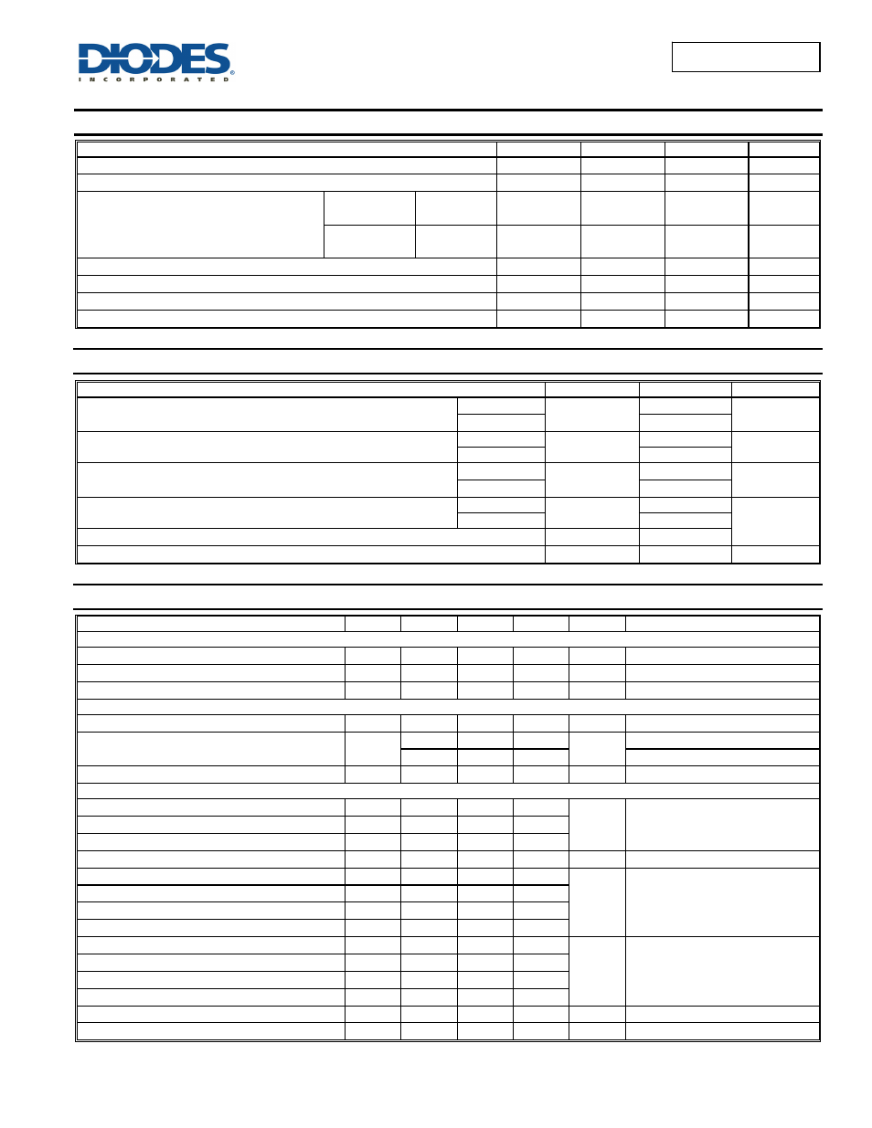
DMC4047LSD
Document number: DS36206 Rev. 4 - 2
2 of 9
November 2013
© Diodes Incorporated
DMC4047LSD
Maximum Ratings
(@T
A
= +25°C, unless otherwise specified.)
Characteristic Symbol
Value_Q2
Value_Q1
Units
Drain-Source Voltage
V
DSS
40 -40 V
Gate-Source Voltage
V
GSS
±20 ±20 V
Continuous Drain Current (Note 6) V
GS
= 10V
Steady
State
T
A
= +25°C
T
A
= +70°C
I
D
7.0
5.6
-5.1
-4.1
A
t<10s
T
A
= +25°C
T
A
= +70°C
I
D
9.0
7.2
-6.5
-5.2
A
Maximum Body Diode Forward Current (Note 6)
I
S
2.5 -2.5 A
Pulsed Drain Current (10µs pulse, duty cycle = 1%)
I
DM
70 -40 A
Avalanche Current (Notes 7) L = 0.1mH
I
AR
20 20 A
Repetitive Avalanche Energy (Notes 7) L = 0.1mH
E
AR
20 20
mJ
Thermal Characteristics
(@T
A
= +25°C, unless otherwise specified.)
Characteristic Symbol
Value
Units
Total Power Dissipation (Note 5)
T
A
= +25°C
P
D
1.3
W
T
A
= +70°C
0.8
Thermal Resistance, Junction to Ambient (Note 5)
Steady state
R
JA
98
°C/W
t<10s 59
Total Power Dissipation (Note 6)
T
A
= +25°C
P
D
1.8
W
T
A
= +70°C
1.1
Thermal Resistance, Junction to Ambient (Note 6)
Steady state
R
θJA
71
°C/W
t<10s 43
Thermal Resistance, Junction to Case (Note 6)
R
θJC
11.8
Operating and Storage Temperature Range
T
J,
T
STG
-55 to +150
°C
Electrical Characteristics N-Channel Q2
(@T
A
= +25°C, unless otherwise specified.)
Characteristic Symbol
Min
Typ
Max
Unit
Test
Condition
OFF CHARACTERISTICS (Note 8)
Drain-Source Breakdown Voltage
BV
DSS
40
V
V
GS
= 0V, I
D
= 250µA
Zero Gate Voltage Drain Current
I
DSS
1 µA
V
DS
= 40V, V
GS
= 0V
Gate-Source Leakage
I
GSS
100
nA
V
GS
= ±20V, V
DS
= 0V
ON CHARACTERISTICS (Note 8)
Gate Threshold Voltage
V
GS(th)
1.4
2.4 V
V
DS
= V
GS
, I
D
= 250µA
Static Drain-Source On-Resistance
R
DS(ON)
15 24
mΩ
V
GS
= 10V, I
D
= 6A
20 32
V
GS
= 4.5V, I
D
= 5A
Diode Forward Voltage
V
SD
0.7 1.0 V
V
GS
= 0V, I
S
= 1.0A
DYNAMIC CHARACTERISTICS (Note 9)
Input Capacitance
C
iss
1060
pF
V
DS
= 20V, V
GS
= 0V,
f = 1.0MHz
Output Capacitance
C
oss
84
Reverse Transfer Capacitance
C
rss
58
Gate Resistance
R
G
1.6
Ω
V
DS
= 0V, V
GS
= 0V, f = 1.0MHz
Total Gate Charge (V
GS
= 4.5V)
Q
g
8.8
nC
V
DS
= 20V, I
D
= 8A
Total Gate Charge (V
GS
= 10V)
Q
g
19.1
Gate-Source Charge
Q
gs
3.0
Gate-Drain Charge
Q
gd
2.5
Turn-On Delay Time
t
D(on)
5.3
nS
V
DD
= 25V, R
L
= 2.5Ω
V
GS
= 10V, R
G
= 3Ω
Turn-On Rise Time
t
r
7.1
Turn-Off Delay Time
t
D(off)
15.1
Turn-Off Fall Time
t
f
4.8
Body Diode Reverse Recovery Time
t
rr
10.5
nS
I
F
= 8A, di/dt = 100A/μs
Body Diode Reverse Recovery Charge
Q
rr
4.15
nC
I
F
= 8A, di/dt = 100A/μs