New prod uc t, Electrical characteristics – q1 n-channel, Typical characteristics – q1 n-channel – Diodes DMC4040SSD User Manual
Page 4: Dmc4040ssd, A product line of diodes incorporated
DMC4040SSD
Document number: DS32120 Rev. 2 - 2
4 of 11
March 2011
© Diodes Incorporated
NEW PROD
UC
T
A Product Line of
Diodes Incorporated
DMC4040SSD
Electrical Characteristics – Q1 N-CHANNEL
@T
A
= 25°C unless otherwise specified
Characteristic Symbol
Min
Typ
Max
Unit
Test
Condition
OFF CHARACTERISTICS
Drain-Source Breakdown Voltage
BV
DSS
40
⎯
⎯
V
I
D
= 250
μA, V
GS
= 0V
Zero Gate Voltage Drain Current
I
DSS
⎯
⎯
1.0
μA
V
DS
= 40V, V
GS
= 0V
Gate-Source Leakage
I
GSS
⎯
⎯
±100
nA
V
GS
=
±20V, V
DS
= 0V
ON CHARACTERISTICS
Gate Threshold Voltage
V
GS(th)
0.8 1.3 1.8 V
I
D
= 250
μA, V
DS
= V
GS
Static Drain-Source On-Resistance (Note 8)
R
DS (ON)
⎯
0.013 0.025
Ω
V
GS
= 10V, I
D
= 3A
0.028 0.040
V
GS
= 4.5V, I
D
= 3A
Forward Transconductance (Notes 8 & 9)
g
fs
⎯
12.6
⎯
S
V
DS
= 5V, I
D
= 3A
Diode Forward Voltage (Note 8)
V
SD
⎯
0.7 1.0 V
I
S
= 1A, V
GS
= 0V
DYNAMIC CHARACTERISTICS (Note 9)
Input Capacitance
C
iss
⎯
1790
⎯
pF
V
DS
= 20V, V
GS
= 0V
f= 1MHz
Output Capacitance
C
oss
⎯
160
⎯
Reverse Transfer Capacitance
C
rss
⎯
120
⎯
Gate Resistance
R
g
⎯
1.03
⎯
Ω
V
DS
= 0V, V
GS
= 0V, f= 1MHz
Total Gate Charge (Note 10)
Q
g
⎯
16.0
⎯
nC
V
GS
= 4.5V
V
DS
= 20V
I
D
= 3A
Total Gate Charge (Note 10)
Q
g
⎯
37.6
⎯
V
GS
= 10V
Gate-Source Charge (Note 10)
Q
gs
⎯
7.8
⎯
Gate-Drain Charge (Note 10)
Q
gd
⎯
6.6
⎯
Turn-On Delay Time (Note 10)
t
D(on)
⎯
8.1
⎯
ns
V
DD
= 20V, V
GS
= 10V
I
D
= 3A
Turn-On Rise Time (Note 10)
t
r
⎯
15.1
⎯
Turn-Off Delay Time (Note 10)
t
D(off)
⎯
24.3
⎯
Turn-Off Fall Time (Note 10)
t
f
⎯
5.3
⎯
Notes:
8. Measured under pulsed conditions. Pulse width
≤ 300μs; duty cycle ≤ 2%
9. For design aid only, not subject to production testing.
10. Switching characteristics are independent of operating junction temperatures.
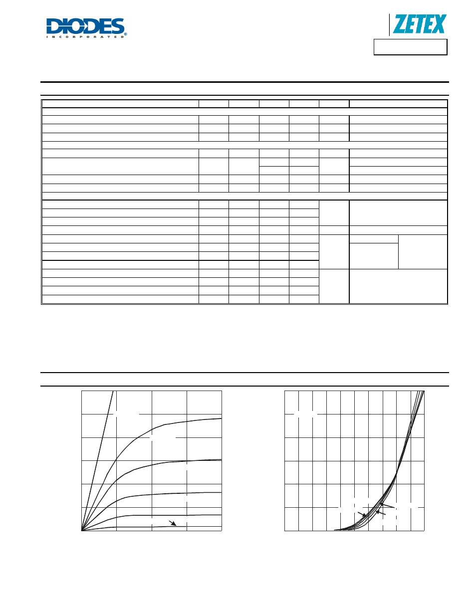
Typical Characteristics – Q1 N-Channel
0
5
10
15
20
25
30
0
0.5
1
1.5
2
Fig. 1 Typical Output Characteristic
V
, DRAIN-SOURCE VOLTAGE (V)
DS
I,
D
R
AI
N
C
U
R
R
EN
T
(A
)
D
V
= 3.5V
GS
V
= 2.5V
GS
V
= 3.0V
GS
V
= 4.0V
GS
V
= 4.5V
GS
V
= 8.0V
GS
0
5
10
15
20
25
30
0
1
2
3
4
5
Fig. 2 Typical Transfer Characteristic
V
, GATE-SOURCE VOLTAGE (V)
GS
I,
D
R
AI
N
C
U
R
R
E
N
T
(A
)
D
T = -55°C
A
T = 25°C
A
T = 85°C
A
T = 125°C
A
T = 150°C
A
V
= 5V
DS