Dmp4050ssd, Electrical characteristics – Diodes DMP4050SSD User Manual
Page 4
DMP4050SSD
Document Number DS32107 Rev 3 - 2
4 of 8
April 2013
© Diodes Incorporated
ADVAN
CE I
N
F
O
RM
ATI
O
N
A Product Line of
Diodes Incorporated
DMP4050SSD
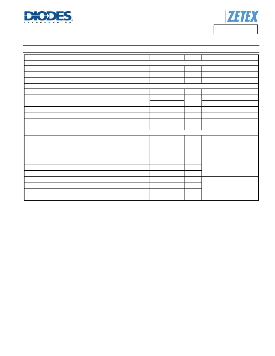
Electrical Characteristics
(@T
A
= +25°C, unless otherwise specified.)
Characteristic Symbol
Min
Typ
Max
Unit
Test
Condition
OFF CHARACTERISTICS
Drain-Source Breakdown Voltage
BV
DSS
-40
V
I
D
= -250µA , V
GS
= 0V
Zero Gate Voltage Drain Current
I
DSS
-0.5 µA
V
DS
= -40V, V
GS
= 0V
Gate-Source Leakage
I
GSS
100
nA
V
GS
=
20V, V
DS
= 0V
ON CHARACTERISTICS
Gate Threshold Voltage
V
GS(th)
-1.0
-3.0 V
I
D
= -250µA, V
DS
= V
GS
Static Drain-Source On-Resistance (Note 12)
R
DS(ON)
0.038 0.050
Ω
V
GS
= -10V, I
D
= -6A
0.055 0.079
V
GS
= -4.5V, I
D
= -5A
Forward Transconductance (Notes 12 & 13)
g
fs
14
S
V
DS
= -15V, I
D
= -6A
Diode Forward Voltage (Note 12)
V
SD
-0.86 -1.2 V
I
S
= -6A, V
GS
= 0V
Reverse recovery time (Note 13)
t
rr
18
ns
I
S
= -2A, di/dt = 100A/µs
Reverse recovery charge (Note 13)
Q
rr
12.7
nC
DYNAMIC CHARACTERISTICS (Note 13)
Input Capacitance
C
iss
674
pF
V
DS
= -20V, V
GS
= 0V
f = 1MHz
Output Capacitance
C
oss
115
pF
Reverse Transfer Capacitance
C
rss
67.7
pF
Total Gate Charge (Note 14)
Q
g
6.9
nC
V
GS
= -4.5V
V
DS
= -20V
I
D
= -6A
Total Gate Charge (Note 14)
Q
g
13.9
nC
V
GS
= -10V
Gate-Source Charge (Note 14)
Q
gs
2
nC
Gate-Drain Charge (Note 14)
Q
gd
3.4
nC
Turn-On Delay Time (Note 14)
t
D(on)
1.9
ns
V
DD
= -20V, V
GS
= -10V
I
D
= -1A, R
G
6.0
Turn-On Rise Time (Note 14)
t
r
3.1
ns
Turn-Off Delay Time (Note 14)
t
D(off)
31.5
ns
Turn-Off Fall Time (Note 14)
t
f
12.6
ns
Notes:
12. Measured under pulsed conditions. Pulse width
300s; duty cycle 2%
13. For design aid only, not subject to production testing.
14. Switching characteristics are independent of operating junction temperatures.