Dms2095lfdb new prod uc t, Electrical characteristics – p-channel mosfet – q1, Electrical characteristics – schottky – d1 – Diodes DMS2095LFDB User Manual
Page 3
DMS2095LFDB
Document number: DS35955 Rev. 3 - 2
3 of 7
April 2014
© Diodes Incorporated
DMS2095LFDB
NEW PROD
UC
T
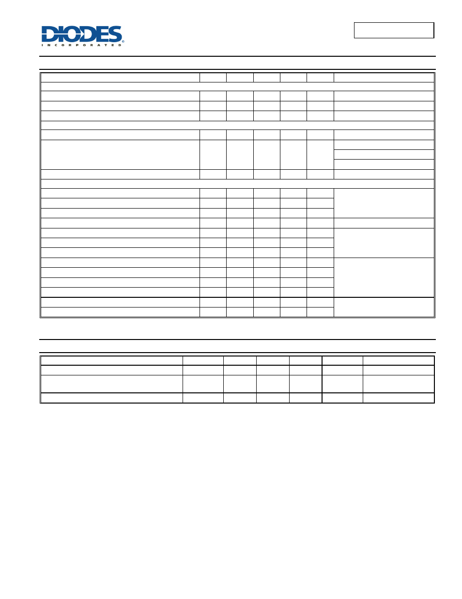
Electrical Characteristics – P-CHANNEL MOSFET – Q1
(@T
A
= +25°C, unless otherwise specified.)
Characteristic Symbol
Min
Typ
Max
Unit
Test
Condition
OFF CHARACTERISTICS (Note 8)
Drain-Source Breakdown Voltage
BV
DSS
-20
⎯
⎯
V
V
GS
= 0V, I
D
= -250μA
Zero Gate Voltage Drain Current
I
DSS
⎯
⎯
-1
μA
V
DS
= -20V, V
GS
= 0V
Gate-Source Leakage
I
GSS
⎯
⎯
±800
nA
V
GS
=
±12V, V
DS
= 0V
ON CHARACTERISTICS (Note 8)
Gate Threshold Voltage
V
GS(th)
-0.4
⎯
-1.3 V
V
DS
= V
GS
, I
D
= -250μA
Static Drain-Source On-Resistance
R
DS (ON)
⎯
⎯
⎯
48
65
90
95
120
150
m
Ω
V
GS
= -4.5V, I
D
= -2.8A
V
GS
= -2.5V, I
D
= -2.0A
V
GS
= -1.8V, I
D
= -1.0A
Diode Forward Voltage
V
SD
⎯
-0.42 -1.2 V V
GS
= 0V, I
S
= -1.0A
DYNAMIC CHARACTERISTICS (Note 9)
Input Capacitance
C
iss
⎯
561
⎯
pF
V
DS
= -10V, V
GS
= 0V
f = 1.0MHz
Output Capacitance
C
oss
⎯
78
⎯
pF
Reverse Transfer Capacitance
C
rss
⎯
66
⎯
pF
Gate Resistance
R
g
⎯
59.5
⎯
Ω
V
DS
= 0V, V
GS
= 0V, f = 1MHz
Total Gate Charge
Q
g
⎯
7.0
⎯
nC
V
GS
= -4.5V, V
DS
= -10V,
I
D
= -2.5A
Gate-Source Charge
Q
gs
⎯
0.9
⎯
nC
Gate-Drain Charge
Q
gd
⎯
1.7
⎯
nC
Turn-On Delay Time
t
D(on)
⎯
5.3
⎯
ns
V
DD
= -10V, V
GS
= -4.5V,
R
L
= 4Ω, R
G
= 6Ω
Turn-On Rise Time
t
r
⎯
5.8
⎯
ns
Turn-Off Delay Time
t
D(off)
⎯
69
⎯
ns
Turn-Off Fall Time
t
f
⎯
54
⎯
ns
Reverse Recovery Time
t
rr
⎯
12.4
⎯
ns
I
F
= -2.5A, di/dt = 100A/μs
Reverse Recovery Charge
Q
rr
⎯
3.7
⎯
nC
Electrical Characteristics – SCHOTTKY – D1
(@T
A
= +25°C, unless otherwise specified.)
Characteristic Symbol
Min
Typ
Max
Unit
Test
Condition
Reverse Breakdown Voltage (Note 8)
V
(BR)R
20 35
⎯
V
I
R
= 1mA
Forward Voltage (Note 8)
V
F
⎯
⎯
—
—
0.40
0.47
V
I
F
= 0.5A
I
F
= 1.0A
Reverse Current (Note 8)
I
R
⎯
30 80 μA
V
R
= 20V
Notes:
8. Short duration pulse test used to minimize self-heating effect.
9. Guaranteed by design. Not subject to product testing