Dms2095lfdb new prod uc t, Maximum ratings – p-channel mosfet – q1, Maximum ratings – schottky – d1 – Diodes DMS2095LFDB User Manual
Page 2: Thermal characteristics
DMS2095LFDB
Document number: DS35955 Rev. 3 - 2
2 of 7
April 2014
© Diodes Incorporated
DMS2095LFDB
NEW PROD
UC
T
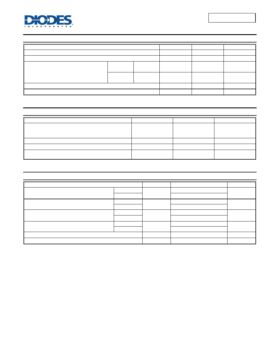
Maximum Ratings – P-CHANNEL MOSFET – Q1
(@T
A
= +25°C, unless otherwise specified.)
Characteristic Symbol
Value
Units
Drain-Source Voltage
V
DSS
-20 V
Gate-Source Voltage (Note 5)
V
GSS
±12 V
Continuous Drain Current (Note 7) V
GS
= -4.5V
Steady
State
T
A
= +25°C
T
A
= +70°C
I
D
-3.4
-2.7
A
t<10s
T
A
= +25°C
T
A
= +70°C
I
D
-3.9
-3.1
A
Maximum Body Diode Forward Current (Note 7)
I
S
-1 A
Pulsed Drain Current (10μs pulse, duty cycle = 1%)
I
DM
-10 A
Maximum Ratings – SCHOTTKY – D1
(@T
A
= +25°C, unless otherwise specified.)
Characteristic Symbol
Value
Unit
Peak Repetitive Reverse Voltage
Working Peak Reverse Voltage
DC Blocking Voltage
V
RRM
V
RWM
V
R
20 V
Average Rectified Output Current (Note 7, t<10s)
I
O
1 A
Peak Repetitive Forward Current (Note 7, t<10s)
I
FRM
2 A
Non-Repetitive Peak Forward Surge Current (Note 7, t<10s)
Single half sine-wave superimposed on rated load
I
FSM
20 A
Thermal Characteristics
(@T
A
= +25°C, unless otherwise specified.)
Characteristic Symbol
Value
Units
Total Power Dissipation (Note 6)
T
A
= +25°C
P
D
0.81
W
T
A
= +70°C
0.52
Thermal Resistance, Junction to Ambient (Note 6)
Steady State
R
θJA
154
°C/W
t<10s 114
Total Power Dissipation (Note 7)
T
A
= +25°C
P
D
1.64
W
T
A
= +70°C
1.04
Thermal Resistance, Junction to Ambient (Note 7)
Steady State
R
θJA
77
°C/W
t<10s 57
Thermal Resistance, Junction to Case (Note 7)
R
θJC
27.5 °C/W
Operating and Storage Temperature Range
T
J,
T
STG
-55 to +150
°C
Notes:
5. AEC-Q101 V
GS
maximum is ±9.6V
6. Device mounted on FR-4 substrate PC board, 2oz copper, with minimum recommended pad layout.
7. Device mounted on FR-4 substrate PC board, 2oz copper, with 1inch square copper plate.