Maximum ratings, Thermal characteristics, Dmp21d0ut – Diodes DMP21D0UT User Manual
Page 2: A product line of diodes incorporated
DMP21D0UT
D
atasheet Number: DS35297 Rev. 2 - 2
2 of 7
March 2012
© Diodes Incorporated
A Product Line of
Diodes Incorporated
DMP21D0UT
Maximum Ratings
@T
A
= 25°C unless otherwise specified
Characteristic
Symbol
Value
Unit
Drain-Source Voltage
V
DSS
-20 V
Gate-Source Voltage
V
GSS
±8 V
Continuous Drain Current
Steady
State
T
A
= 25°C (Note 4)
T
A
= 85°C (Note 4)
T
A
= 25°C (Note 5)
I
D
-0.59
-0.42
-0.65
A
Pulsed Drain Current (Note 6)
I
DM
-5.0 A
Thermal Characteristics
@T
A
= 25°C unless otherwise specified
Characteristic Symbol
Value
Unit
Power Dissipation (Note 4)
P
D
0.24 W
Power Dissipation (Note 5)
P
D
0.33 W
Thermal Resistance, Junction to Ambient (Note 4)
R
θJA
525 °C/W
Thermal Resistance, Junction to Ambient (Note 5)
R
θJA
383 °C/W
Operating and Storage Temperature Range
T
J
,
T
STG
-55 to +150
°C
Notes:
4. Device mounted on FR-4 substrate PC board, 2oz copper, with minimum recommended pad layout
5. Device mounted on 25mm X 25mm FR-4 PCB with high coverage of 2oz copper
6. Device mounted on minimum recommended pad layout test board, 10
μs pulse duty cycle = 1%.
0.0001
0.001
0.01
0.1
1
10
100
1,000
t , PULSE DURATION TIME (SEC)
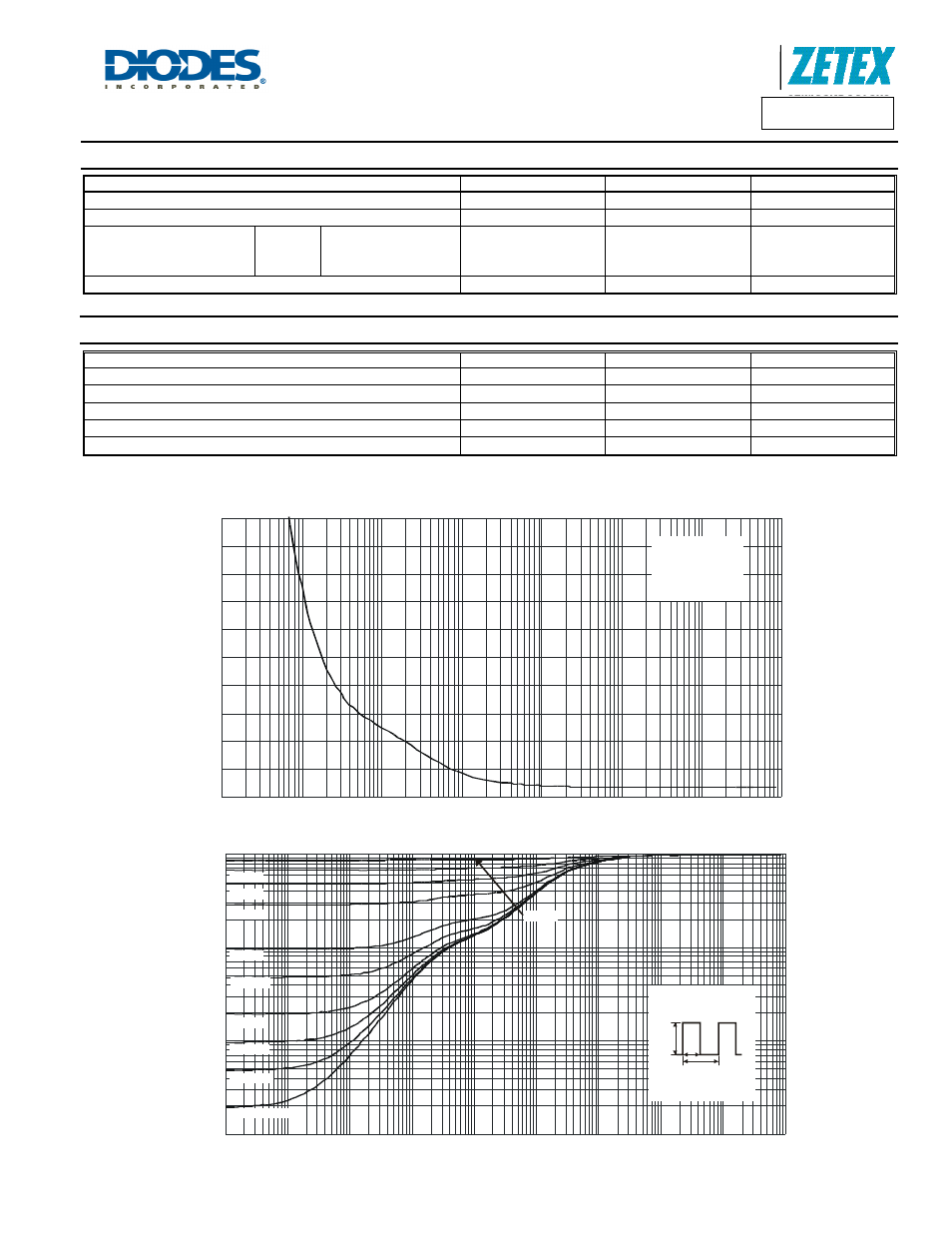
Fig. 1 Single Pulse Maximum Power Dissipation
1
0
1
2
3
4
5
6
7
8
9
10
P
(p
k
),
P
EAK
T
R
A
N
SI
EN
T
P
O
WE
R
(W
)
Single Pulse
R
= 380°C/W
R
(t) = r(t) * R
T - T = P * R
(t)
θ
θ
θ
θ
JA
JA
JA
J
A
JA
0.000001 0.00001
0.0001
0.001
0.01
0.1
1
10
100
1,000
Fig. 2 Transient Thermal Response
t , PULSE DURATION TIME (s)
1
0.001
0.01
0.1
1
r(
t),
T
R
A
N
SI
EN
T
T
H
E
R
MA
L
R
ES
IS
T
AN
C
E
T - T = P * R
(t)
Duty Cycle, D = t /t
J
A
JA
1 2
θ
R
(t) = r(t) *
θJA
R
R
= 380°C/W
θ
θ
JA
JA
P(pk)
t
1
t
2
D = 0.7
D = 0.5
D = 0.3
D = 0.1
D = 0.05
D = 0.02
D = 0.01
D = 0.005
D = Single Pulse
D = 0.9