Diodes DMP21D0UT User Manual
Dmp21d0ut, Product summary, Description and applications
DMP21D0UT
D
atasheet Number: DS35297 Rev. 2 - 2
1 of 7
March 2012
© Diodes Incorporated
A Product Line of
Diodes Incorporated
DMP21D0UT
20V P-CHANNEL ENHANCEMENT MODE MOSFET
Product Summary
V
(BR)DSS
R
DS(on)
Max
I
D
Max
@ T
A
= 25
°C
(Note 4)
-20V
495m
Ω @ V
GS
= -4.5V
-0.59A
690m
Ω @ V
GS
= -2.5V
-0.50A
960m
Ω @ V
GS
= -1.8V
-0.42A
Description and Applications
This MOSFET has been designed to minimize the on-state resistance
(R
DS(on)
) and yet maintain superior switching performance, making it
ideal for high efficiency power management applications.
• Portable
electronics
Features and Benefits
•
Footprint of just 3mm
2
– less than half the size of SOT23
•
0.8mm profile – ideal for low profile applications
•
Low Gate Threshold Voltage
•
Fast Switching Speed
•
ESD Protected Gate 3KV
•
Totally Lead-Free & Fully RoHS compliant (Note 1)
•
Halogen and Antimony Free. “Green” Device (Note 2)
•
Qualified to AEC-Q101 Standards for High Reliability
Mechanical Data
• Case:
SOT523
•
Case Material: Molded Plastic, “Green” Molding Compound.
UL Flammability Classification Rating 94V-0
•
Moisture Sensitivity: Level 1 per J-STD-020
•
Terminals: Matte Tin Finish ; Solderable per MIL-STD-202,
Method 208
•
Weight: 0.002 grams (approximate)
Ordering Information
(Note 3)
Part Number
Marking
Reel size (inches)
Tape width (mm)
Quantity per reel
DMP21D0UT-7 PBC
7
8
3,000
Notes:
1. EU Directive 2002/95/EC (RoHS) & 2011/65/EU (RoHS 2) compliant. No purposely added lead. Halogen and Antimony free.
2. Diodes Inc's "Green" policy can be found on our w
3. For packaging details, go to our website at
Marking Information
Date Code Key
Year
2011
2012
2013
2014
2015
2016
2017
Code Y
Z
A
B
C D
E
Month
Jan
Feb
Mar
Apr
May
Jun
Jul
Aug
Sep
Oct
Nov
Dec
Code 1 2 3 4 5 6 7 8 9 O N D
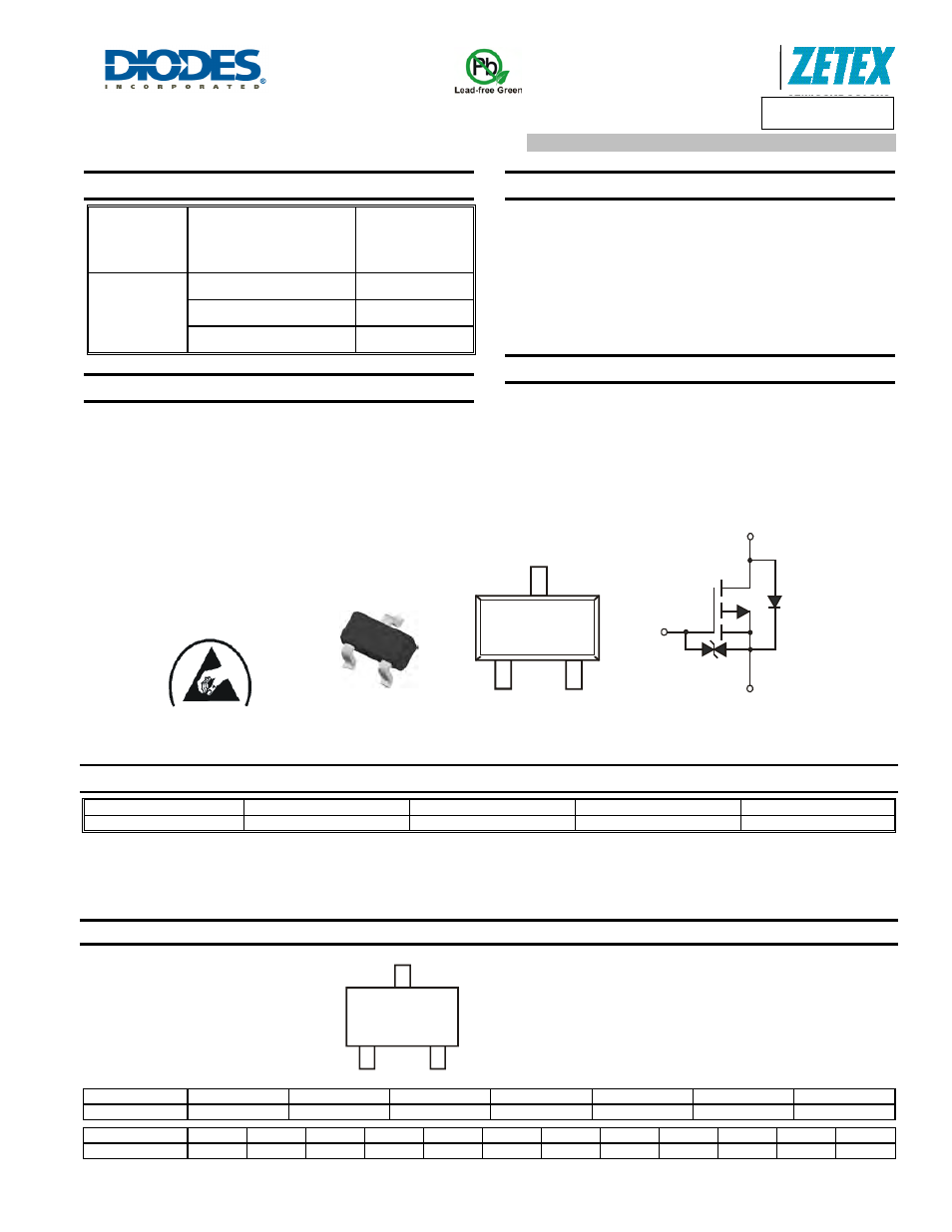
SOT523
Equivalent Circuit
Top View
Internal Schematic
Bottom View
Source
Gate
Protection
Diode
Gate
Drain
G
S
D
ESD PROTECTED TO 3kV
PBC
YM
PBC = Product Type Marking Code
YM = Date Code Marking
Y = Year (ex: Y = 2011)
M = Month (ex: 9 = September)