Maximum ratings, Thermal characteristics, Electrical characteristics – Diodes DMP2039UFDE User Manual
Page 2: Dmp2039ufde
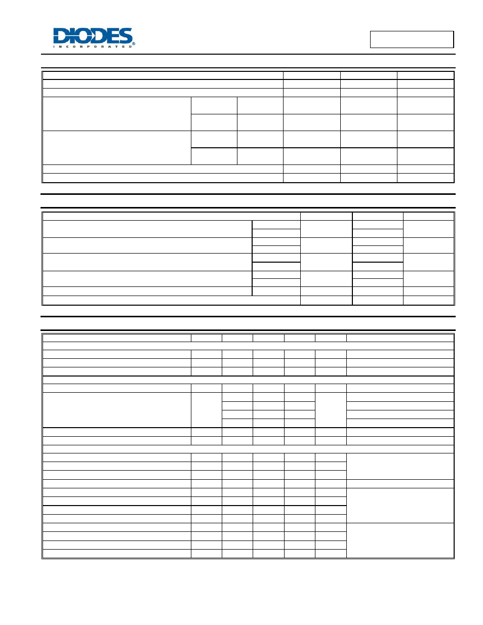
DMP2039UFDE
Document number: DS35420 Rev. 5 - 2
2 of 6
July 2012
© Diodes Incorporated
DMP2039UFDE
Maximum Ratings
(@T
A
= +25°C, unless otherwise specified.)
Characteristic Symbol
Value
Units
Drain-Source Voltage
V
DSS
-25 V
Gate-Source Voltage
V
GSS
±8 V
Continuous Drain Current (Note 5) V
GS
= -4.5V
Steady
State
T
A
= +25°C
T
A
= +70°C
I
D
-6.7
-5.3
A
t<5s
T
A
= +25°C
T
A
= +70°C
I
D
-8.3
-6.6
A
Continuous Drain Current (Note 5) V
GS
= -1.8V
Steady
State
T
A
= +25°C
T
A
= +70°C
I
D
-5.4
-4.3
A
t<5s
T
A
= +25°C
T
A
= +70°C
I
D
-6.6
-5.2
A
Pulsed Drain Current (10µs pulse, duty cycle = 1%)
I
DM
-60 A
Continuous Source-Drain Diode Current
I
S
-2.0 A
Thermal Characteristics
Characteristic Symbol
Value
Units
Total Power Dissipation (Note 5)
T
A
= +25°C
P
D
0.8
W
T
A
= +70°C
1.2
Thermal Resistance, Junction to Ambient (Note 5)
Steady state
R
θJA
160
°C/W
t<5s 104
Total Power Dissipation (Note 6)
T
A
= +25°C
P
D
2.0
W
T
A
= +70°C
2.9
Thermal Resistance, Junction to Ambient (Note 6)
Steady state
R
θJA
63
°C/W
t<5s 42
Thermal Resistance, Junction to Case (Note 6)
Steady state
R
θJC
10.8 °C/W
Operating and Storage Temperature Range
T
J,
T
STG
-55 to +150
°C
Electrical Characteristics
(@T
A
= +25°C, unless otherwise specified.)
Characteristic Symbol
Min
Typ
Max
Unit
Test
Condition
OFF CHARACTERISTICS (Note 7)
Drain-Source Breakdown Voltage
BV
DSS
-25
⎯
⎯
V
V
GS
= 0V, I
D
= -250µA
Zero Gate Voltage Drain Current
I
DSS
⎯
⎯
-1 µA
V
DS
= -25V, V
GS
= 0V
Gate-Source Leakage
I
GSS
⎯
⎯
±10
µA
V
GS
=
±8.0V, V
DS
= 0V
ON CHARACTERISTICS (Note 7)
Gate Threshold Voltage
V
GS(th)
-0.4
⎯
-1.0 V
V
DS
= V
GS
, I
D
= -250µA
Static Drain-Source On-Resistance
R
DS (ON)
⎯
20 27
m
Ω
V
GS
= -4.5V, I
D
= -6.4A
⎯
24 34
V
GS
= -2.5V, I
D
= -4.8A
⎯
28 40
V
GS
= -1.8V, I
D
= -2.5A
⎯
33 70
V
GS
= -1.5V, I
D
= -1.5A
Forward Transfer Admittance
|Y
fs
|
⎯
16
⎯
S
V
DS
= -5V, I
D
= -4A
Diode Forward Voltage
V
SD
⎯
-0.7 -1.0 V
V
GS
= 0V, I
S
= -1A
DYNAMIC CHARACTERISTICS (Note 8)
Input Capacitance
C
iss
⎯
2530
⎯
pF
V
DS
= -15V, V
GS
= 0V
f = 1.0MHz
Output Capacitance
C
oss
⎯
203
⎯
pF
Reverse Transfer Capacitance
C
rss
⎯
177
⎯
pF
Gate Resistance
R
g
⎯
9.1
⎯
Ω
V
DS
= 0V, V
GS
= 0V, f = 1.0MHz
Total Gate Charge (V
GS
= -4.5V)
Q
g
⎯
28.2
⎯
nC
V
DS
= -15V, I
D
= -4.0A
Total Gate Charge (V
GS
= -8V
Q
g
⎯
48.7
⎯
nC
Gate-Source Charge
Q
gs
⎯
3.2
⎯
nC
Gate-Drain Charge
Q
gd
⎯
5.0
⎯
nC
Turn-On Delay Time
t
D(on)
⎯
15.1
⎯
ns
V
DD
= -15V, V
GS
= -4.5V, R
G
= 1
Ω,
I
D
= -4.0A
Turn-On Rise Time
t
r
⎯
23.5
⎯
ns
Turn-Off Delay Time
t
D(off)
⎯
137.6
⎯
ns
Turn-Off Fall Time
t
f
⎯
80.5
⎯
ns
Notes:
5. Device mounted on FR-4 PC board, with minimum recommended pad layout, single sided.
6. Device mounted on FR-4 substrate PC board, 2oz copper, with thermal bias to bottom layer 1inch square copper plate
7. Short duration pulse test used to minimize self-heating effect
8. Guaranteed by design. Not subject to production testing.