Maximum ratings, Thermal characteristics, Dmp1022ufde – Diodes DMP1022UFDE User Manual
Page 2
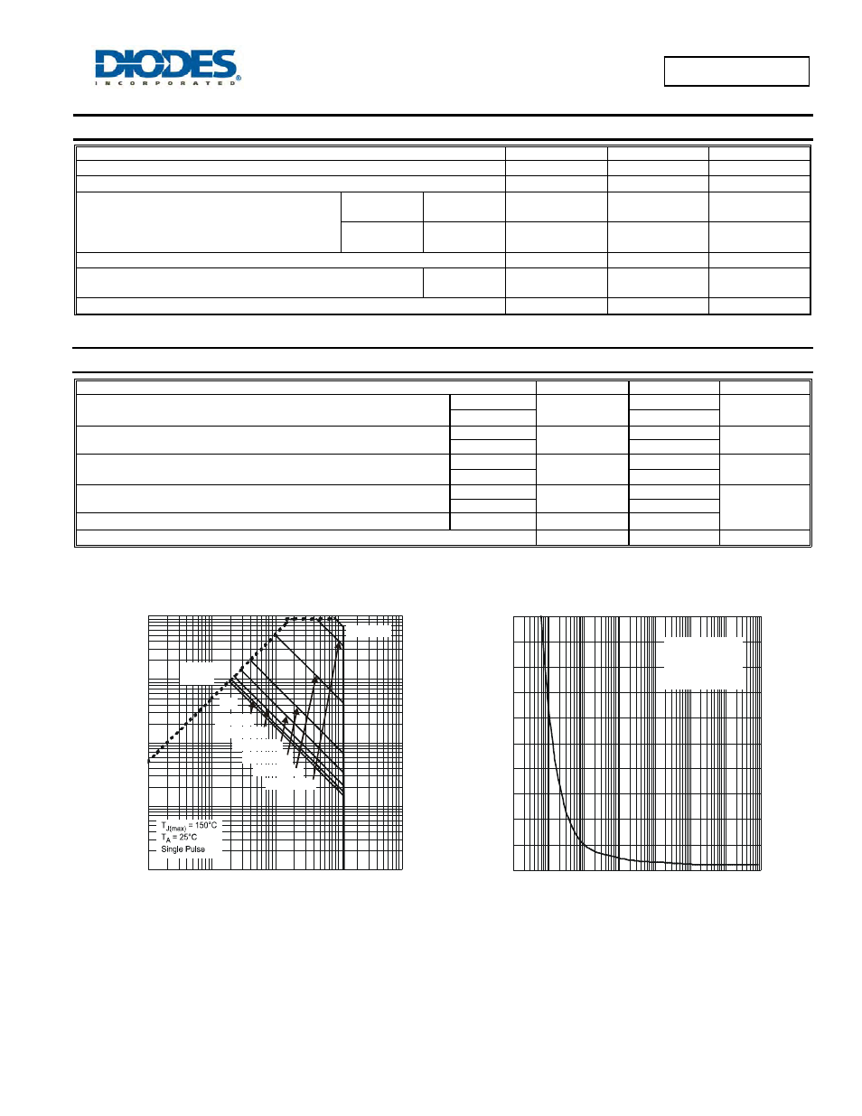
DMP1022UFDE
D
atasheet number: DS35477 Rev. 9 - 2
2 of 7
July 2012
© Diodes Incorporated
DMP1022UFDE
Maximum Ratings
(@T
A
= +25°C, unless otherwise specified.)
Characteristic Symbol
Value
Units
Drain-Source Voltage
V
DSS
-12 V
Gate-Source Voltage
V
GSS
±8 V
Continuous Drain Current (Note 6) V
GS
= -4.5V
Steady
State
T
A
= +25°C
T
A
= +70°C
I
D
-9.1
-7.2
A
t<5s
T
A
= +25°C
T
A
= +70°C
I
D
-11.2
-9.0
A
Pulsed Drain Current (10
μs pulse, duty cycle = 1%)
I
DM
-90 A
Continuous Source-Drain Diode Current
T
A
= +25°C
T
C
= +25°C
I
S
-2.5
-7.1
A
Pulsed Source-Drain Diode Current (10
μs pulse, duty cycle = 1%)
I
SM
-50 A
Thermal Characteristics
Characteristic Symbol
Value
Units
Total Power Dissipation (Note 5)
T
A
= +25°C
P
D
0.66
W
T
A
= +70°C
0.42
Thermal Resistance, Junction to Ambient (Note 5)
Steady state
R
θJA
189
°C/W
t<5s 123
Total Power Dissipation (Note 6)
T
A
= +25°C
P
D
2.03
W
T
A
= +70°C
1.3
Thermal Resistance, Junction to Ambient (Note 6)
Steady state
R
θJA
61
°C/W
t<5s 40
Thermal Resistance, Junction to Case (Note 6)
Steady state
R
θJC
9.3
Operating and Storage Temperature Range
T
J,
T
STG
-55 to +150
°C
Notes:
5. Device mounted on FR-4 PC board, with minimum recommended pad layout, single sided.
6. Device mounted on FR-4 substrate PC board, 2oz copper, with thermal vias to bottom layer 1inch square copper plate
0.01
0.1
1
10
100
0.01
0.1
1
10
100
-V
, DRAIN-SOURCE VOLTAGE (V)
Fig. 1 SOA, Safe Operation Area
DS
-I
, D
R
AI
N
C
U
R
R
EN
T
(A
)
D
R
Limited
DS(on)
DC
P = 10s
W
P = 1s
W
P = 100ms
W
P = 10ms
W
P = 1ms
W
P = 100µs
W
P = 10 s
W
µ
0
10
20
30
40
50
60
70
80
90
100
t1, PULSE DURATION TIME (sec)
Fig. 2 Single Pulse Maximum Power Dissipation
0.001 0.01
0.1
1
10
100
1,000
0.0001
P
,
P
EAK
T
R
ANSI
EN
T
P
O
IW
E
R
(W
)
(P
K
)
Single Pulse
R
= 61 C/W
R
= r
* R
T - T = P * R
θ
θ
θ
θ
JA
JA(t)
(t)
JA
J
A
JA(t)
°