Dmn65d8lfb, Dmn65d8lfb new prod uc t, Maximum ratings – Diodes DMN65D8LFB User Manual
Page 2: Thermal characteristics, Electrical characteristics
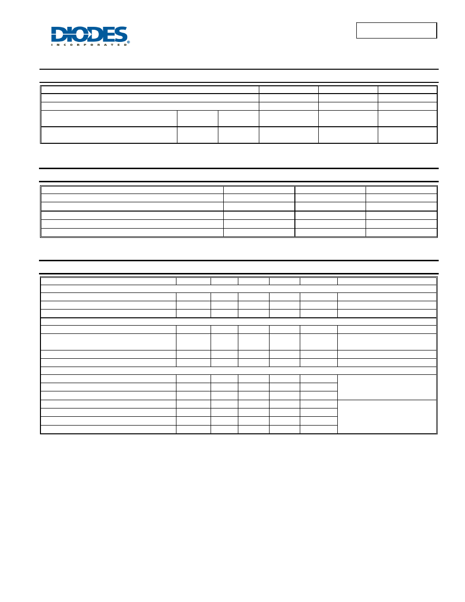
DMN65D8LFB
Document number: DS35449 Rev. 2 - 2
2 of 5
November 2011
© Diodes Incorporated
DMN65D8LFB
NEW PROD
UC
T
Maximum Ratings
Characteristic Symbol
Value
Units
Drain-Source Voltage
V
DSS
60 V
Gate-Source Voltage
V
GSS
±20
V
Continuous Drain Current (Note 4) V
GS
= 10V
Steady
State
T
A
= 25°C
T
A
= 70°C
I
D
260
210
mA
Continuous Drain Current (Note 5) V
GS
= 10V
Steady
State
T
A
= 25°C
T
A
= 70°C
I
D
400
310
mA
Thermal Characteristics
Characteristic Symbol
Value
Units
Power Dissipation, @T
A
= 25°C (Note 4)
P
D
430 mW
Thermal Resistance, Junction to Ambient @T
A
= 25°C (Note 4)
R
θJA
290
°C/W
Power Dissipation, @T
A
= 25°C (Note 5)
P
D
840 mW
Thermal Resistance, Junction to Ambient @T
A
= 25°C (Note 5)
R
θJSA
147
°C/W
Operating and Storage Temperature Range
T
J
, T
STG
-55 to +150
°C
Electrical Characteristics
@T
A
= 25°C unless otherwise specified
Characteristic Symbol
Min
Typ
Max
Unit
Test
Condition
OFF CHARACTERISTICS (Note 6)
Drain-Source Breakdown Voltage
BV
DSS
60 - -
V
V
GS
= 0V, I
D
= 250
μA
Zero Gate Voltage Drain Current T
J
= 25°C
I
DSS
- - 0.1 µA
V
DS
= 60V, V
GS
= 0V
Gate-Body Leakage
I
GSS
- -
±10
µA
V
GS
=
±20V, V
DS
= 0V
ON CHARACTERISTICS (Note 6)
Gate Threshold Voltage
V
GS(th)
1.2 - 2.0 V
V
DS
= V
GS
, I
D
= 250
μA
Static Drain-Source On-Resistance
R
DS (ON)
-
-
3.0
4.0
Ω
V
GS
= 10V, I
D
= 0.115A
V
GS
= 5V, I
D
= 0.1115A
Forward Transfer Admittance
|Y
fs
|
80 320 -
mS
V
DS
= 10V, I
D
= 0.115A
Diode Forward Voltage
V
SD
- 0.7 1.2 V
V
GS
= 0V, I
S
= 0.115A
DYNAMIC CHARACTERISTICS (Note 7)
Input Capacitance
C
iss
- 25 - pF
V
DS
= 25V, V
GS
= 0V, f = 1.0MHz
Output Capacitance
C
oss
- 4.7 -
pF
Reverse Transfer Capacitance
C
rss
- 2.5 -
pF
Turn-On Delay Time
t
D(on)
- 3.27 -
ns
V
DD
= 30V, V
GEN
= 10V,
R
GEN
= 25
Ω,I
D
= 0.115A
Turn-On Rise Time
t
r
- 3.15 -
ns
Turn-Off Delay Time
t
D(off)
- 12.025 -
ns
Turn-Off Fall Time
t
f
- 6.29 -
ns
Notes:
4. Device mounted on FR-4 PCB with minimum recommended pad layout, single sided.
5. Device mounted on 2” x 2” FR-4 PCB with high coverage 2 oz. Copper, single sided.
6. Short duration pulse test used to minimize self-heating effect.
7. Guaranteed by design. Not subject to production testing.