Dmn62d0sfd new prod uc t, Maximum ratings, Thermal characteristics – Diodes DMN62D0SFD User Manual
Page 2: Electrical characteristics, Dmn62d0sfd
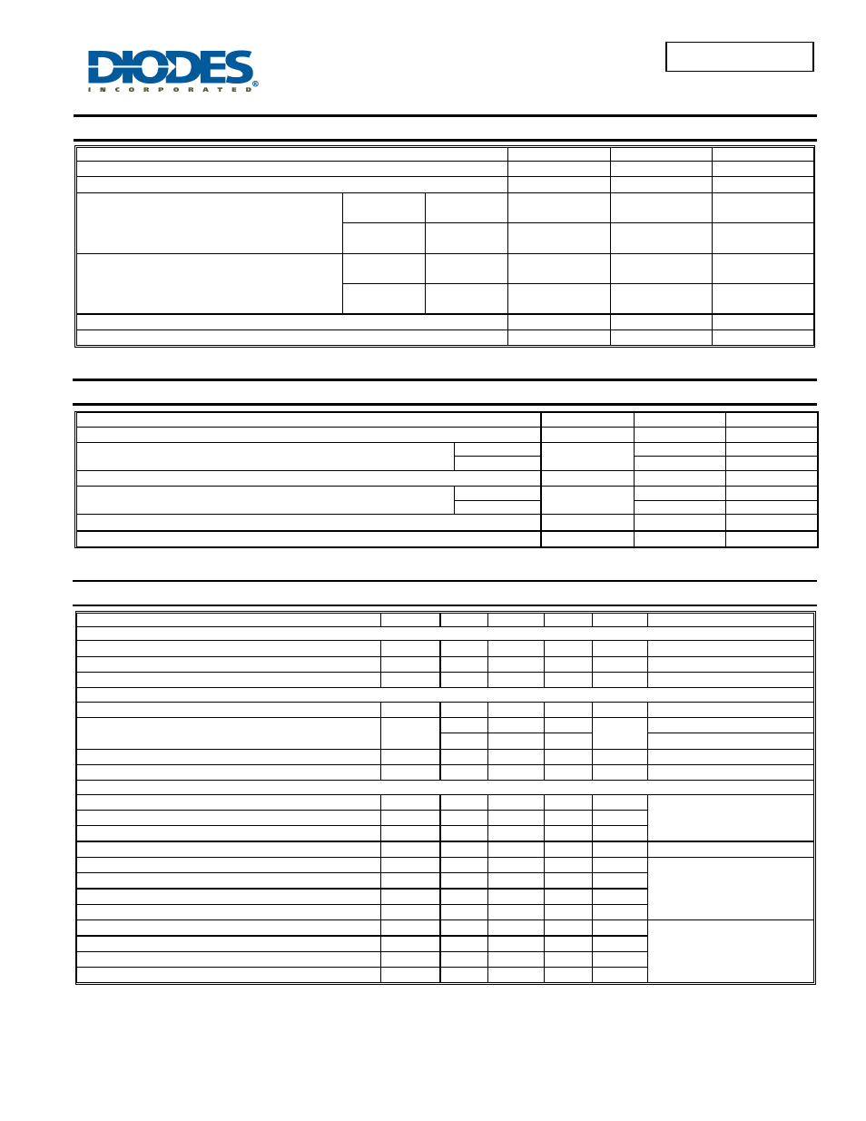
DMN62D0SFD
Document number: DS35473 Rev. 3 - 2
2 of 6
January 2012
© Diodes Incorporated
DMN62D0SFD
NEW PROD
UC
T
Maximum Ratings
@T
A
= 25°C unless otherwise specified
Characteristic Symbol
Value
Units
Drain-Source Voltage
V
DSS
60 V
Gate-Source Voltage
V
GSS
±20 V
Continuous Drain Current (Note 5) V
GS
= 10V
Steady
State
T
A
= 25°C
T
A
= 70°C
I
D
540
430
mA
t<10s
T
A
= 25°C
T
A
= 70°C
I
D
630
500
mA
Continuous Drain Current (Note 5) V
GS
= 5V
Steady
State
T
A
= 25°C
T
A
= 70°C
I
D
430
340
mA
t<10s
T
A
= 25°C
T
A
= 70°C
I
D
510
410
mA
Pulsed Drain Current (10
μs pulse, duty cycle = 1%)
I
DM
1.0 A
Maximum Body Diode Forward Current (Note 5)
I
S
1.0 A
Thermal Characteristics
@T
A
= 25°C unless otherwise specified
Characteristic Symbol
Value
Units
Total Power Dissipation (Note 4)
P
D
0.43 W
Thermal Resistance, Junction to Ambient (Note 4)
Steady state
R
θJA
260 °C/W
t<10s 182
°C/W
Total Power Dissipation (Note 5)
P
D
0.89 W
Thermal Resistance, Junction to Ambient (Note 5)
Steady state
R
θJA
140 °C/W
t<10s 98
°C/W
Thermal Resistance, Junction to Case (Note 5)
R
θJC
112 °C/W
Operating and Storage Temperature Range
T
J,
T
STG
-55 to +150
°C
Electrical Characteristics
@T
A
= 25°C unless otherwise specified
Characteristic
Symbol
Min
Typ
Max
Unit
Test Condition
OFF CHARACTERISTICS (Note 6)
Drain-Source Breakdown Voltage
BV
DSS
60 - - V
V
GS
= 0V, I
D
= 10
μA
Zero Gate Voltage Drain Current T
J
= 25°C
I
DSS
- -
100
nA
V
DS
= 60V, V
GS
= 0V
Gate-Source Leakage
I
GSS
- - 10
μA
V
GS
= ±20V, V
DS
= 0V
ON CHARACTERISTICS (Note 6)
Gate Threshold Voltage
V
GS(th)
1.0 1.6 2.5 V
V
DS
= 10V, I
D
= 1mA
Static Drain-Source On-Resistance
R
DS (ON)
- - 2 Ω
V
GS
= 10V, I
D
= 500mA
- - 3
V
GS
= 5V, I
D
= 50mA
Forward Transfer Admittance
|Y
fs
|
- 130 - mS
V
DS
= 3V, I
D
= 30mA
Diode Forward Voltage
V
SD
- 0.8
1.2 V
V
GS
= 0V, I
S
= 300mA
DYNAMIC CHARACTERISTICS (Note 7)
Input Capacitance
C
iss
- 30.2 - pF
V
DS
= 25V, V
GS
= 0V,
f = 1.0MHz
Output Capacitance
C
oss
- 4.4 - pF
Reverse Transfer Capacitance
C
rss
- 2.8 - pF
Gate Resistance
R
g
- 131 -
Ω
V
DS
= 0V, V
GS
= 0V, f = 1MHz
Total Gate Charge (V
GS
= 4.5V)
Q
g
- 0.39 - nC
V
DS
= 10V, I
D
= 1A
Total Gate Charge (V
GS
= 10.0V)
Q
g
- 0.87 - nC
Gate-Source Charge
Q
gs
- 0.14 - nC
Gate-Drain Charge
Q
gd
- 0.09 - nC
Turn-On Delay Time
t
D(on)
- 3.95 - ns
V
DS
= 30V, I
D
= 200mA
V
GS
= 10V, R
G
= 25Ω
Turn-On Rise Time
t
r
- 3.81 - ns
Turn-Off Delay Time
t
D(off)
- 16.0 - ns
Turn-Off Fall Time
t
f
- 9.04 - ns
Notes:
4. Device mounted on FR-4 PC board, with minimum recommended pad layout, single sided.
5. Device mounted on FR-4 substrate PC board, 2oz copper, with thermal vias to bottom layer 1inch square copper plate
6 .Short duration pulse test used to minimize self-heating effect.
7. Guaranteed by design. Not subject to production testing.