Diodes DMN62D0LFB User Manual
Product summary, Description and applications, Features and benefits
DMN62D0LFB
Document number: DS35409 Rev. 2 - 2
1 of 6
October 2011
© Diodes Incorporated
DMN62D0LFB
ADVAN
CE I
N
F
O
RM
ATI
O
N
NEW PROD
UC
T
N-CHANNEL ENHANCEMENT MODE MOSFET
Product Summary
V
(BR)DSS
R
DS(ON)
I
D
T
A
= 25°C
60V
2
Ω @ V
GS
= 4V
100mA
2.5
Ω @ V
GS
= 2.5V
50mA
Description and Applications
This new generation MOSFET has been designed to minimize the on-
state resistance (R
DS(on)
) and yet maintain superior switching
performance, making it ideal for high efficiency power management
applications.
• DC-DC
Converters
•
Power management functions
•
Battery Operated Systems and Solid-State Relays
•
Drivers: Relays, Solenoids, Lamps, Hammers, Displays,
Memories, Transistors, etc.
Features and Benefits
• Low
On-Resistance
•
Low Input Capacitance
•
Fast Switching Speed
•
Low Input/Output Leakage
•
ESD Protected
•
Lead Free By Design/RoHS Compliant (Note 1)
•
"Green" Device (Note 2)
•
Qualified to AEC-Q101 Standards for High Reliability
Mechanical Data
• Case:
X1-DFN1006-3
•
Case Material: Molded Plastic, "Green" Molding Compound. UL
Flammability Classification Rating 94V-0
•
Moisture Sensitivity: Level 1 per J-STD-020
• Terminals:
Finish
⎯ NiPdAu over Copper leadframe. Solderable
per MIL-STD-202, Method 208
•
Weight: 0.001 grams (approximate)
Ordering Information
(Note 3)
Product
Marking
Reel size (inches)
Tape width (mm)
Quantity per reel
DMN62D0LFB-7 NK
7
8
3,000
DMN62D0LFB-7B NK
7
8
10,000
Notes: 1. No purposefully added lead.
2. Diodes Inc.'s "Green" policy can be found on our w3. For packaging details, go to our website at
Marking Information
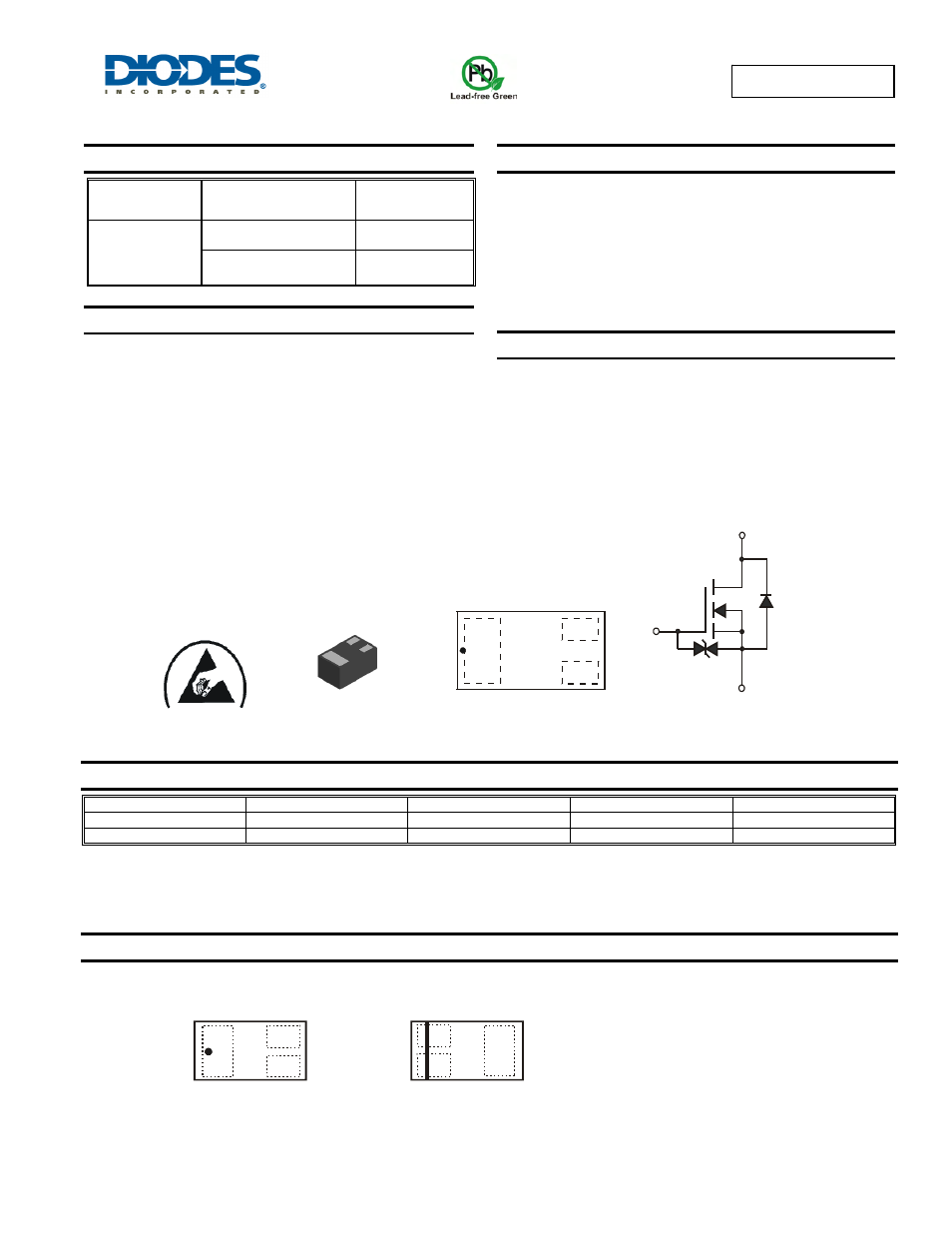
X1-DFN1006-3
Bottom View
Top View
Pin-Out
Source
Gate
Protection
Diode
Gate
Drain
Equivalent Circuit
ESD PROTECTED
D
S
G
NK = Product Type Marking Code
Top View
Dot Denotes Drain Side
DMN62D0LFB-7
Top View
Bar Denotes Gate and Source Side
DMN62D0LFB-7B
NK
NK