Diodes DMN62D0LFD User Manual
Product summary, Description, Applications
DMN62D0LFD
Document number: DS36359 Rev. 2 - 2
1 of 6
May 2014
© Diodes Incorporated
DMN62D0LFD
ADVAN
CE I
N
F
O
RM
ATI
O
N
NEW PROD
UC
T
NEW PROD
UC
T
N-CHANNEL ENHANCEMENT MODE MOSFET
Product Summary
V
(BR)DSS
R
DS(ON)
I
D
T
A
= +25°C
60V
2Ω @ V
GS
= 4V
310mA
2.5Ω @ V
GS
= 2.5V
295mA
Description
This new generation MOSFET has been designed to minimize the on-
state resistance (R
DS(ON)
) and yet maintain superior switching
performance, making it ideal for high efficiency power management
applications.
Applications
• DC-DC
Converters
•
Power management functions
•
Battery Operated Systems and Solid-State Relays
•
Drivers: Relays, Solenoids, Lamps, Hammers, Displays,
Memories, Transistors, etc.
Features and Benefits
• Low
On-Resistance
•
Low Input Capacitance
•
Fast Switching Speed
•
Low Input/Output Leakage
•
ESD Protected
•
Totally Lead-Free & Fully RoHS Compliant (Notes 1 & 2)
•
Halogen and Antimony Free. “Green” Device (Note 3)
•
Qualified to AEC-Q101 Standards for High Reliability
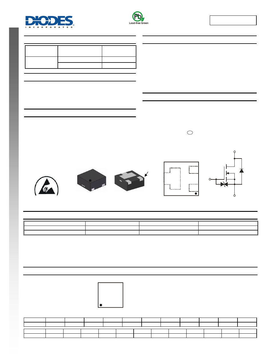
Mechanical Data
• Case:
X1-DFN1212-3
•
Case Material: Molded Plastic. UL Flammability Classification
Rating 94V-0
•
Moisture Sensitivity: Level 1 per J-STD-020
•
Terminals: NiPdAu over Copper leadframe. Solderable per MIL-
STD-202, Method 208
•
Terminal Connections: See Diagram
•
Weight: 0.005 grams (approximate)
Ordering Information
(Note 4)
Part Number
Compliance Case
Packaging
DMN62D0LFD
-7 Standard X1-DFN1212-3
3,000/Tape
&
Reel
DMN62D0LFD
-13
Standard
X1-DFN1212-3
10,000/Tape & Reel
Notes:
1. No purposely added lead. Fully EU Directive 2002/95/EC (RoHS) & 2011/65/EU (RoHS 2) compliant.
2. S more information about Diodes Incorporated’s definitions of Halogen- and Antimony-free, "Green"
and Lead-free.
3. Halogen- and Antimony-free "Green” products are defined as those which contain <900ppm bromine, <900ppm chlorine (<1500ppm total Br + Cl) and
<1000ppm antimony compounds.
4. For packaging details, go to our website at
Marking Information
Date Code Key
Year
2007
2008
2009
2010 2011 2012 2013 2014 2015 2016 2017
Code
U V W X Y Z A B C D E
Month
Jan
Feb
Mar
Apr
May
Jun
Jul
Aug
Sep
Oct
Nov
Dec
Code 1 2 3 4 5 6 7 8 9 O N D
Top View
Bottom View
Source
Body
Diode
Gate
Protection
Diode
Gate
Drain
Equivalent Circuit
ESD PROTECTED
K63 = Product Type Marking Code
YM = Date Code Marking
Y = Year (ex: Y = 2013)
M = Month (ex: 9 = September)
G pin
K63
YM
Pin-Out Top View
D
S
G
e4