Electrical characteristics, Dmn6040svt – Diodes DMN6040SVT User Manual
Page 3
DMN6040SVT
Document number: DS35562 Rev. 10 - 2
3 of 7
March 2012
© Diodes Incorporated
DMN6040SVT
ADVAN
CE I
N
F
O
RM
ATI
O
N
0.00001
0.0001
0.001
0.01
0.1
1
10
100
1,000
t1, PULSE DURATION TIME (sec)
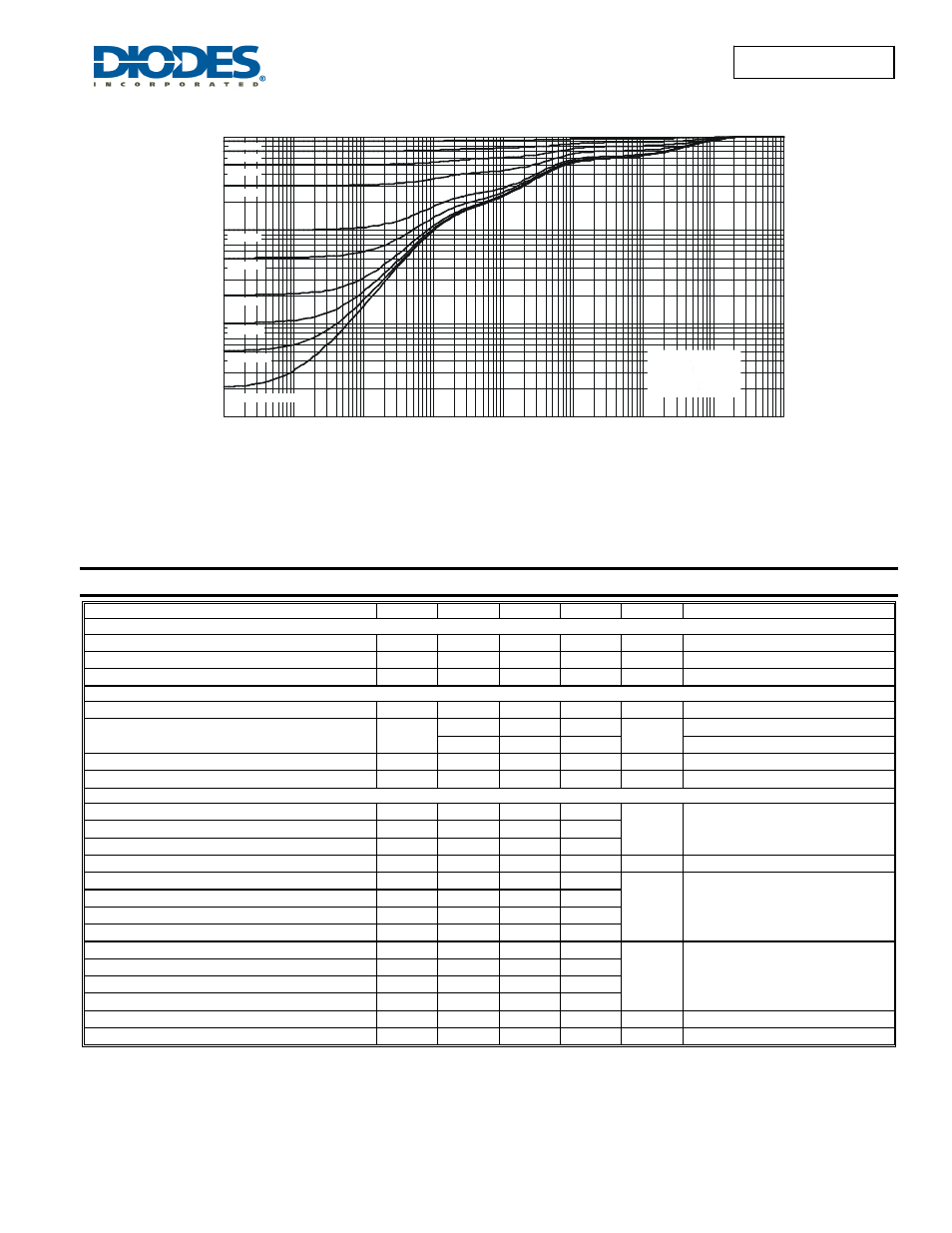
Fig. 3 Transient Thermal Resistance
0.001
0.01
0.1
1
r(t
),
T
R
AN
SI
EN
T
T
H
E
R
MA
L
R
ES
IS
T
AN
C
E
R
= r
* R
θJA(t)
(t)
θ
θ
JA
JA
R
= 72 C/W
Duty Cycle, D = t1/t2
°
D = 0.5
D = 0.7
D = 0.9
D = 0.3
D = 0.1
D = 0.05
D = 0.02
D = 0.01
D = 0.005
D = Single Pulse
Electrical Characteristics
@T
A
= 25°C unless otherwise specified
Characteristic Symbol
Min
Typ
Max
Unit
Test
Condition
OFF CHARACTERISTICS (Note 7)
Drain-Source Breakdown Voltage
BV
DSS
60
⎯
⎯
V
V
GS
= 0V, I
D
= 250
μA
Zero Gate Voltage Drain Current
I
DSS
⎯
⎯
100 nA
V
DS
= 60V, V
GS
= 0V
Gate-Source Leakage
I
GSS
⎯
⎯
±100
nA
V
GS
=
±20V, V
DS
= 0V
ON CHARACTERISTICS (Note 7)
Gate Threshold Voltage
V
GS(th)
1
⎯
3 V
V
DS
= V
GS
, I
D
= 250
μA
Static Drain-Source On-Resistance
R
DS (ON)
⎯
30 44
m
Ω
V
GS
= 10V, I
D
= 4.3A
⎯
35 60
V
GS
= 4.5V, I
D
= 4A
Forward Transfer Admittance
|Y
fs
|
⎯
4.5
⎯
S
V
DS
= 10V, I
D
= 4.3A
Diode Forward Voltage
V
SD
⎯
0.7 1.2 V
V
GS
= 0V, I
S
= 1A
DYNAMIC CHARACTERISTICS (Note 8)
Input Capacitance
C
iss
⎯
1287
⎯
pF
V
DS
= 25V, V
GS
= 0V
f = 1.0MHz
Output Capacitance
C
oss
⎯
57
⎯
Reverse Transfer Capacitance
C
rss
⎯
44
⎯
Gate Resistance
R
G
⎯
1.2
⎯
Ω
V
DS
= 0V, V
GS
= 0V, f = 1.0MHz
Total Gate Charge (V
GS
= 10V)
Q
g
⎯
22.4
⎯
nC
V
DS
= 30V, I
D
= 4.3A
Total Gate Charge (V
GS
= 4.5V)
Q
g
⎯
10.4
⎯
Gate-Source Charge
Q
gs
⎯
4.9
⎯
Gate-Drain Charge
Q
gd
⎯
3.0
⎯
Turn-On Delay Time
t
D(on)
⎯
6.6
⎯
nS
V
GS
= 10V, V
DD
= 30V, R
G
= 6
Ω,
I
D
= 4.3A
Turn-On Rise Time
t
r
⎯
8.1
⎯
Turn-Off Delay Time
t
D(off)
⎯
20.1
⎯
Turn-Off Fall Time
t
f
⎯
4.0
⎯
Body Diode Reverse Recovery Time
t
rr
⎯
18
⎯
nS
I
S
= 4.3A, dI/dt = 100A/
μs
Body Diode Reverse Recovery Charge
Q
rr
⎯
11.9
⎯
nC
I
S
= 4.3A, dI/dt = 100A/
μs
Notes:
4. Device mounted on FR-4 substrate PC board, 2oz copper, with minimum recommended pad layout.
5. Device mounted on FR-4 substrate PC board, 2oz copper, with 1inch square copper plate.
6. I
AR
and E
AR
rating are based on low frequency and duty cycles to keep T
J
= 25°C
7. Short duration pulse test used to minimize self-heating effect.
8. Guaranteed by design. Not subject to product testing.