Maximum ratings, Thermal characteristics, Electrical characteristics – Diodes DMG8880LK3 User Manual
Page 2
DMG8880LK3
Document number: DS32052 Rev. 4 - 2
2 of 6
December 2010
© Diodes Incorporated
DMG8880LK3
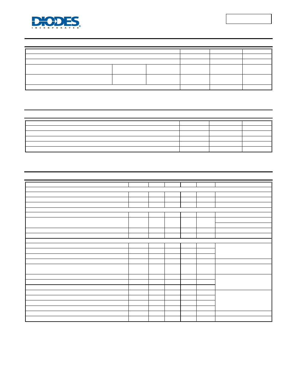
Maximum Ratings
@T
A
= 25°C unless otherwise specified
Characteristic
Symbol
Value
Unit
Drain-Source Voltage
V
DSS
30 V
Gate-Source Voltage
V
GSS
±20 V
Continuous Drain Current (Note 4) V
GS
= 10V
Steady
State
T
A
= 25°C
T
A
= 85°C
I
D
11
8
A
Continuous Drain Current (Note 5) V
GS
= 10V
Steady
State
T
A
= 25°C
T
A
= 85°C
I
D
16.5
12
A
Pulsed Drain Current (Note 6)
I
DM
48 A
Thermal Characteristics
Characteristic Symbol
Value
Unit
Power Dissipation (Note 4)
P
D
1.68 W
Thermal Resistance, Junction to Ambient @T
A
= 25°C (Note 4)
R
θJA
74.3 °C/W
Power Dissipation (Note 5)
P
D
4.1 W
Thermal Resistance, Junction to Ambient @T
A
= 25°C (Note 5)
R
θJA
30.8 °C/W
Operating and Storage Temperature Range
T
J
,
T
STG
-55 to +150
°C
Electrical Characteristics
@T
A
= 25°C unless otherwise specified
Characteristic
Symbol
Min
Typ
Max
Unit
Test Condition
OFF CHARACTERISTICS (Note 7)
Drain-Source Breakdown Voltage
BV
DSS
30 - - V
V
GS
= 0V, I
D
= 250
μA
Zero Gate Voltage Drain Current T
J
= 25°C
I
DSS
- -
1.0
μA
V
DS
= 30V, V
GS
= 0V
Gate-Source Leakage
I
GSS
- -
±100
nA
V
GS
= ±20V, V
DS
= 0V
ON CHARACTERISTICS (Note 7)
Gate Threshold Voltage
V
GS(th)
1.2 1.5 2.3 V V
DS
= V
GS
, I
D
= 250
μA
Static Drain-Source On-Resistance
R
DS (ON)
-
5
8
7.5
12
mΩ
V
GS
= 10V, I
D
= 11.6A
V
GS
= 4.5V, I
D
= 10.7A
Forward Transfer Admittance
|Y
fs
|
- 22 - S
V
DS
= 15V, I
D
= 15A
Diode Forward Voltage
V
SD
- 0.7
1.0 V
V
GS
= 0V, I
SD
= 2.1A
DYNAMIC CHARACTERISTICS (Note 8)
Input Capacitance
C
iss
- 1289 - pF
V
DS
= 15V, V
GS
= 0V,
f = 1.0MHz
Output Capacitance
C
oss
- 187 - pF
Reverse Transfer Capacitance
C
rss
- 162 - pF
Gate Resistance
R
g
- 0.97 - Ω
V
DS
= 0V, V
GS
= 0V, f = 1MHz
Total Gate Charge at 10V
Q
g
- 27.6 - nC
V
GS
= 10V, V
DS
= 15V,
I
D
= 11.6A, Ig = 1.0mA
Total Gate Charge at 5V
Q
g
- 14.4 - nC
V
GS
= 5V, V
DS
= 15V,
I
D
= 11.6A
Gate-Source Charge
Q
gs
- 3.6 - nC
Gate-Drain Charge
Q
gd
- 4.9 - nC
Turn-On Delay Time
t
D(on)
- 7.04 - ns
V
DD
= 15V, V
GS
= 10V,
R
G
= 11
Ω, I
D
= 11.6A,
R
L
= 1.3
Ω
Turn-On Rise Time
t
r
- 17.52 -
ns
Turn-Off Delay Time
t
D(off)
- 36.13 -
ns
Turn-Off Fall Time
t
f
- 19.67 -
ns
Body Diode Reverse Recovery Time
t
rr
- 17.6 - ns
I
F
= 20A, dl/dt = 500A/
μs
Body Diode Reverse Recovery Charge
Q
rr
- 65.9 - nC
I
F
= 20A, dl/dt = 500A/
μs
Notes:
4. Device mounted on FR-4 PCB, with minimum recommended pad layout, single sided.
5. Device mounted on 2” x 2” FR-4 PCB with high coverage 2oz. copper, single sided.
6.
Repetitive rating, pulse width limited by junction temperature and current limited by package.
7. Short duration pulse test used to minimize self-heating effect.
8. Guaranteed by design. Not subject to production testing.