Package outline dimensions, Suggested pad layout – Diodes DMG4468LK3 User Manual
Page 5
DMG4468LK3
Document number: DS31958 Rev. 3 - 2
5 of 6
June 2013
© Diodes Incorporated
DMG4468LK3
NE
W
P
R
OD
UC
T
Package Outline Dimensions
Please see AP02002 at latest version.
Suggested Pad Layout
Please see AP02001 at the latest version.
0.001
0.01
0.1
1
0.00001
0.0001
0.001
0.01
0.1
1
10
100
1,000
r(t
),
T
R
AN
S
IEN
T
T
H
ER
M
A
L
R
ES
IST
AN
C
E
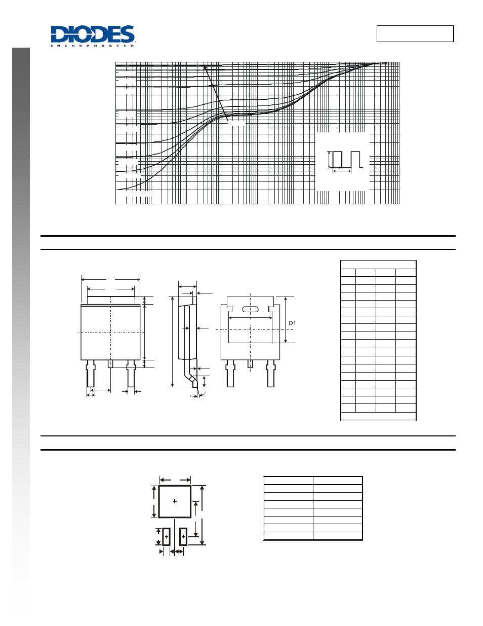
Fig. 13 Transient Thermal Response
t , PULSE DURATION TIME (s)
1
T - T = P * R
(t)
Duty Cycle, D = t /t
J
A
JA
1 2
θ
R
(t) = r(t) *
θJA
R
R
= 76°C/W
θ
θ
JA
JA
P(pk)
t
1
t
2
D = 0.7
D = 0.5
D = 0.3
D = 0.1
D = 0.05
D = 0.02
D = 0.01
D = 0.005
D = Single Pulse
D = 0.9
TO252
Dim Min
Max
Typ
A
2.19
2.39
2.29
A1 0.00
0.13
0.08
A2 0.97
1.17
1.07
b
0.64
0.88 0.783
b2
0.76
1.14
0.95
b3
5.21
5.46
5.33
c2
0.45
0.58 0.531
D
6.00
6.20
6.10
D1 5.21
−
−
e
−
−
2.286
E
6.45
6.70
6.58
E1 4.32
−
−
H
9.40 10.41 9.91
L
1.40
1.78
1.59
L3
0.88
1.27
1.08
L4
0.64
1.02
0.83
a
0°
10°
−
All Dimensions in mm
Dimensions
Value (in mm)
Z
11.6
X1
1.5
X2
7.0
Y1
2.5
Y2
7.0
C
6.9
E1
2.3
X2
C
Z
X1
Y1
E1
Y2
b3
E
2X b2
D
L4
A
c2
e
A1
L
L3
3X b
a
H
A2
E1