Diodes DMN26D0UT User Manual
Dmn26d0ut new prod uc t, Features, Mechanical data
DMN26D0UT
Document number: DS31854 Rev. 2 - 2
1 of 6
September 2009
© Diodes Incorporated
DMN26D0UT
NEW PROD
UC
T
N-CHANNEL ENHANCEMENT MODE MOSFET
Features
• Low
On-Resistance:
• 3.0
Ω @ 4.5V
• 4.0
Ω @ 2.5V
• 6.0
Ω @ 1.8V
• 10
Ω @ 1.5V
•
Very Low Gate Threshold Voltage, 1.0V max
•
Low Input Capacitance
•
Fast Switching Speed
•
Low Input/Output Leakage
•
Ultra-Small Surface Mount Package
• ESD
Protected
Gate
•
Lead, Halogen, and Antimony Free By Design/RoHS
Compliant (Note 2)
•
"Green" Device (Note 3)
•
Qualified to AEC-Q101 Standards for High Reliability
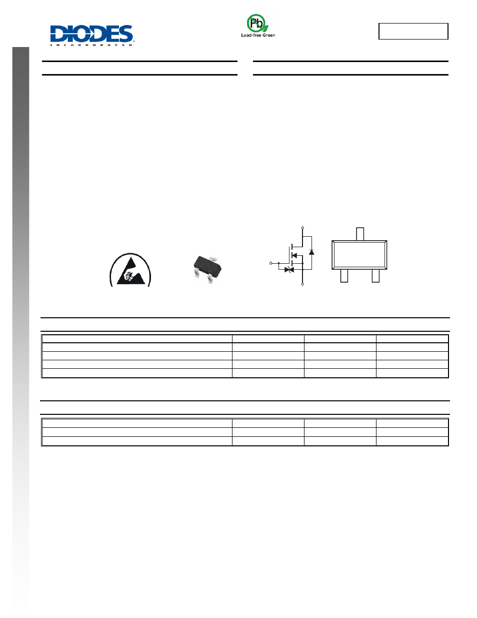
Mechanical Data
• Case:
SOT-523
•
Case Material: Molded Plastic, “Green” Molding Compound. UL
Flammability Classification Rating 94V-0
•
Moisture Sensitivity: Level 1 per J-STD-020
•
Terminal Connections: See Diagram
•
Terminals: Finish – Matte Tin annealed over Alloy 42 leadframe.
Solderable per MIL-STD-202, Method 208
•
Marking Information: See Page 4
•
Ordering Information: See Page 4
•
Weight: 0.002 grams (approximate)
Maximum Ratings
@T
A
= 25°C unless otherwise specified
Characteristic Symbol
Value
Unit
Drain Source Voltage
V
DSS
20 V
Gate-Source Voltage
V
GSS
±10
V
Drain Current (Note 1)
I
D
230 mA
Pulsed Drain Current T
P
= 10µs
I
DM
805 mA
Thermal Characteristics
@T
A
= 25°C unless otherwise specified
Total Power Dissipation (Note 1)
P
D
300 mW
Thermal Resistance, Junction to Ambient (Note 1)
R
θJA
417
°C/W
Operating and Storage Temperature Range
T
J
, T
STG
-55 to +150
°C
Notes:
1. Device mounted on FR-4 PCB, 1 inch x 0.85 inch x 0.062 inch; pad layout as shown on Diodes Inc. suggested pad layout document AP02001, which
can be found on our website
2. No purposefully added lead.
3. Diodes Inc.’s “Green” policy can be found on our websit
TOP VIEW
EQUIVALENT CIRCUIT
TOP VIEW
Source
Gate
Protection
Diode
Gate
Drain
G
S
D
ESD PROTECTED