Maximum ratings, Thermal characteristics, Electrical characteristics – Diodes DMN26D0UFB4 User Manual
Page 2: Dmn26d0ufb4
DMN26D0UFB4
Document number: DS31775 Rev. 7 - 2
2 of 6
March 2012
© Diodes Incorporated
DMN26D0UFB4
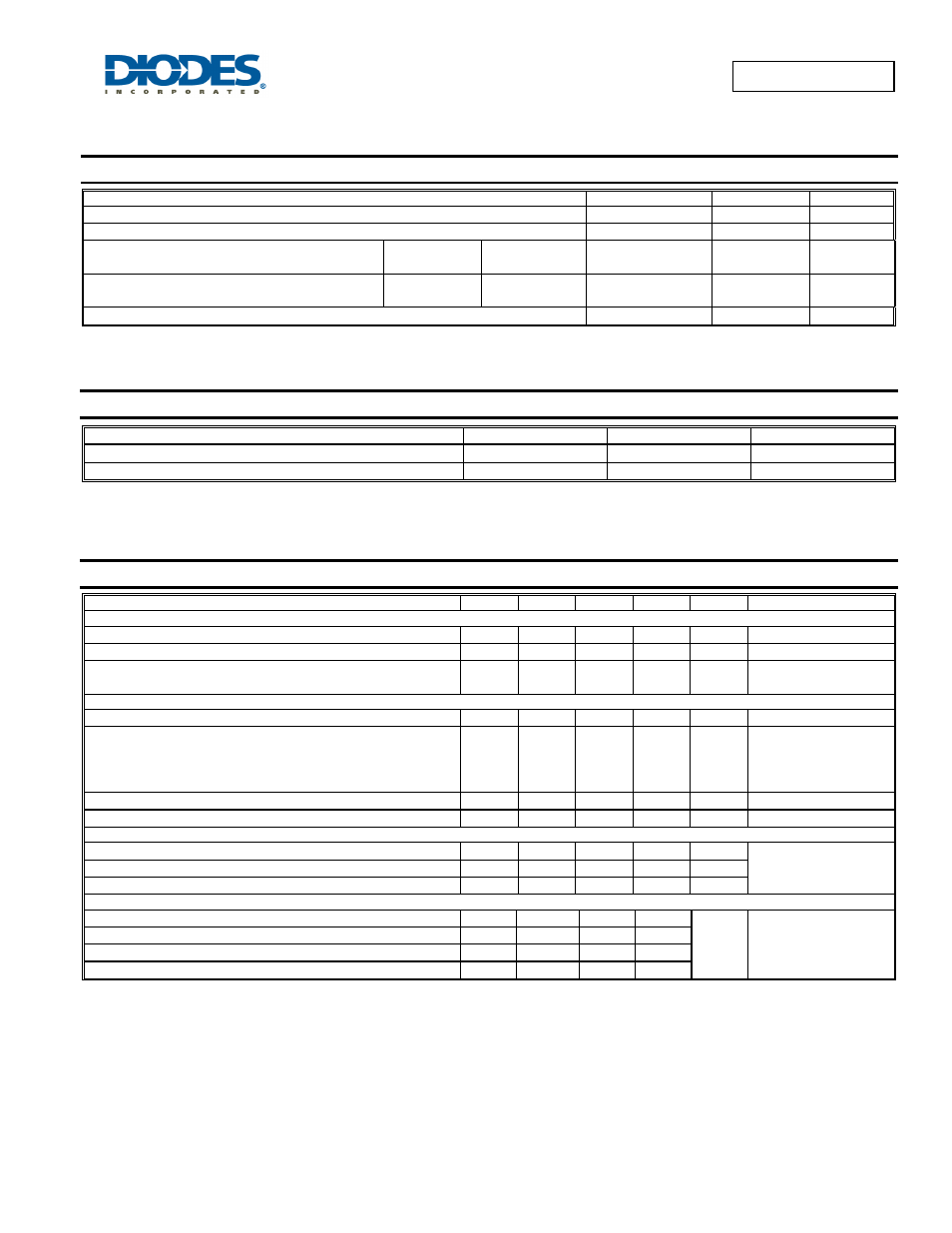
Maximum Ratings
@T
A
= 25°C unless otherwise specified
Characteristic Symbol
Value
Unit
Drain Source Voltage
V
DSS
20 V
Gate-Source Voltage
V
GSS
±10
V
Continuous Drain Current (Note 4) V
GS
= 4.5V
Steady
State
T
A
= 25°C
T
A
= 70°C
I
D
240
190
mA
Continuous Drain Current (Note 4) V
GS
= 1.8V
Steady
State
T
A
= 25°C
T
A
= 70°C
I
D
180
140
mA
Pulsed Drain Current - T
P
= 10µs
I
DM
805 mA
Thermal Characteristics
@T
A
= 25°C unless otherwise specified
Total Power Dissipation (Note 4) @T
A
= 25°C
P
D
350 mW
Thermal Resistance, Junction to Ambient (Note 4)
R
θJA
357
°C/W
Operating and Storage Temperature Range
T
J
, T
STG
-55 to +150
°C
Electrical Characteristics
@T
A
= 25°C unless otherwise specified
Characteristic Symbol
Min
Typ
Max
Unit
Test
Condition
OFF CHARACTERISTICS (Note 5)
Drain-Source Breakdown Voltage
BV
DSS
20
⎯
⎯
V
V
GS
= 0V, I
D
= 100
μA
Zero Gate Voltage Drain Current @ T
C
= 25°C
I
DSS
⎯
⎯
500 nA
V
DS
= 20V, V
GS
= 0V
Gate-Body Leakage
I
GSS
⎯
⎯
±1
±100
μA
nA
V
GS
= ±10V, V
DS
= 0V
V
GS
= ±5V, V
DS
= 0V
ON CHARACTERISTICS (Note 5)
Gate Threshold Voltage
V
GS(th)
0.45
⎯
1.05 V
V
DS
= V
GS
, I
D
= 250
μA
Static Drain-Source On-Resistance
R
DS (ON)
⎯
⎯
⎯
⎯
1.8
2.5
3.4
4.7
3.0
4.0
6.0
10.0
Ω
V
GS
= 4.5V, I
D
= 100mA
V
GS
= 2.5V, I
D
= 50mA
V
GS
= 1.8V, I
D
= 20mA
V
GS
= 1.5V, I
D
= 10mA
Forward Transconductance
|Y
fs
|
180 242
⎯
mS
V
DS
= 10V, I
D
= 0.1A
Source-Drain Diode Forward Voltage
V
SD
0.5
⎯
1.4 V
V
GS
= 0V, I
S
= 115mA
DYNAMIC CHARACTERISTICS
Input Capacitance
C
iss
⎯
14.1
⎯
pF
V
DS
= 15V, V
GS
= 0V
f = 1.0MHz
Output Capacitance
C
oss
⎯
2.9
⎯
pF
Reverse Transfer Capacitance
C
rss
⎯
1.6
⎯
pF
SWITCHING CHARACTERISTICS
Turn-On Delay Time
t
d(on)
⎯
3.8
⎯
ns
V
GS
= 4.5V, V
DD
= 10V
I
D
= 200mA, R
G
= 2.0
Ω
Rise Time
t
r
⎯
7.9
⎯
Turn-Off Delay Time
t
d(off)
⎯
13.4
⎯
Fall Time
t
f
⎯
15.2
⎯
Notes:
4. Device mounted on FR-4 PC board, with minimum recommended pad layout, single sided.
5.
Short duration pulse test used to minimize self-heating effect.