Electrical characteristics, Dmn2300ufd, A product line of diodes incorporated – Diodes DMN2300UFD User Manual
Page 3
DMN2300UFD
Datasheet Number: DS35443 Rev. 2 - 2
3 of 7
September 2011
© Diodes Incorporated
A Product Line of
Diodes Incorporated
DMN2300UFD
0.00001
0.0001
0.001
0.01
0.1
1
10
100
1,000
t1, PULSE DURATION TIMES (sec)
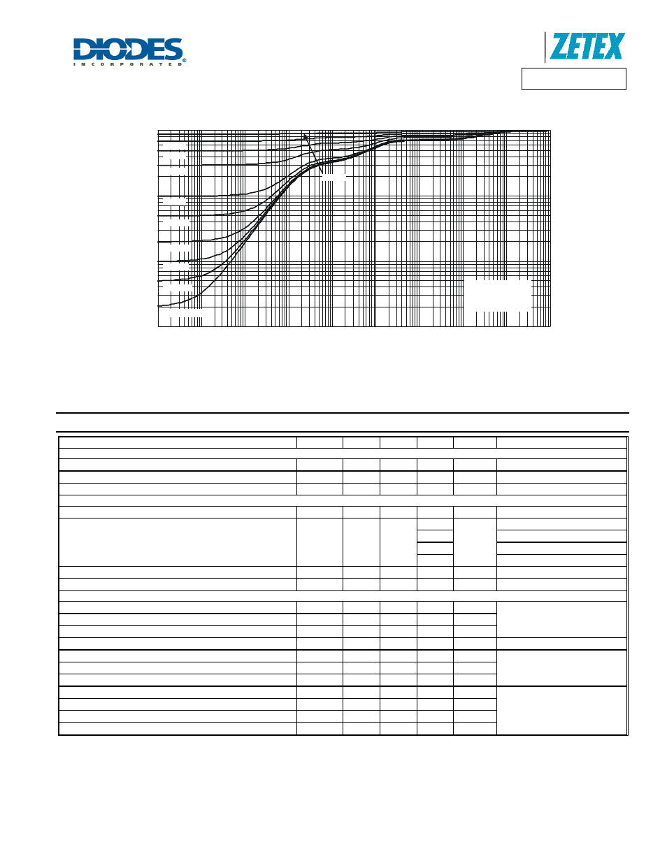
Fig. 3 Transient Thermal Resistance
0.000001
0.001
0.01
0.1
1
r(t),
T
R
ANSI
E
N
T
T
H
E
R
MA
L
R
ES
IS
T
AN
C
E
R
(t) = r(t) * R
θ
θ
JA
JA
R
= 136°C/W
Duty Cycle, D = t1/ t2
θJA
D = 0.7
D = 0.5
D = 0.3
D = 0.1
D = 0.05
D = 0.02
D = 0.01
D = 0.005
D = Single Pulse
D = 0.9
Electrical Characteristics
@T
A
= 25°C unless otherwise specified
Characteristic
Symbol
Min
Typ
Max
Unit
Test Condition
OFF CHARACTERISTICS (Note 7)
Drain-Source Breakdown Voltage
BV
DSS
20 - - V
V
GS
= 0V, I
D
= 250
μA
Zero Gate Voltage Drain Current T
J
= 25°C
I
DSS
- - 1
μA
V
DS
= 20V, V
GS
= 0V
Gate-Source Leakage
I
GSS
- -
±10
μA
V
GS
= ±8V, V
DS
= 0V
ON CHARACTERISTICS (Note 7)
Gate Threshold Voltage
V
GS(th)
0.45 - 0.95 V
V
DS
= V
GS
, I
D
= 250
μA
Static Drain-Source On-Resistance
R
DS (ON)
- -
200
m
Ω
V
GS
= 4.5V, I
D
= 900mA
260
V
GS
= 2.5V, I
D
= 800mA
400
V
GS
= 1.8V, I
D
= 700mA
500
V
GS
= 1.5V, I
D
= 200mA
Forward Transfer Admittance
|Y
fs
|
40 - - mS
V
DS
= 3V, I
D
= 300mA
Diode Forward Voltage
V
SD
- 0.7
1.2 V
V
GS
= 0V, I
S
= 300mA
DYNAMIC CHARACTERISTICS
Input Capacitance
C
iss
- 67.62 -
pF
V
DS
= 25V, V
GS
= 0V,
f = 1.0MHz
Output Capacitance
C
oss
- 9.74 - pF
Reverse Transfer Capacitance
C
rss
- 7.58 - pF
Gate Resistance
R
g
- 68.51 -
Ω
V
DS
= 0V, V
GS
= 0V, f = 1MHz
Total Gate Charge (Note 8)
Q
g
- 0.89 2 nC
V
GS
= 4.5V, V
DS
= 15V,
I
D
= 1A
Gate-Source Charge
Q
gs
- 0.14 - nC
Gate-Drain Charge
Q
gd
- 0.16 - nC
Turn-On Delay Time
t
D(on)
- 4.92 - ns
V
DS
= 10V, I
D
= 1A
V
GS
= 10V, R
G
= 6Ω
Turn-On Rise Time
t
r
- 6.93 - ns
Turn-Off Delay Time
t
D(off)
- 21.71 -
ns
Turn-Off Fall Time
t
f
- 10.62 -
ns
Notes:
7. Short duration pulse test used to minimize self-heating effect.
8. Guarantee by design.