Maximum ratings, Thermal characteristics, Dmn2300ufd – Diodes DMN2300UFD User Manual
Page 2: A product line of diodes incorporated
DMN2300UFD
Datasheet Number: DS35443 Rev. 2 - 2
2 of 7
September 2011
© Diodes Incorporated
A Product Line of
Diodes Incorporated
DMN2300UFD
Maximum Ratings
@T
A
= 25°C unless otherwise specified
Characteristic
Symbol
Value
Unit
Drain-Source Voltage
V
DSS
20 V
Gate-Source Voltage
V
GSS
±8 V
Continuous Drain Current
Steady
State
T
A
= 25°C (Note 4)
I
D
1.73
A
T
A
= 85°C (Note 4)
1.34
T
A
= 25°C (Note 5)
1.21
Pulsed Drain Current (Note 6)
I
DM
6.0 A
Thermal Characteristics
@T
A
= 25°C unless otherwise specified
Characteristic Symbol
Value
Unit
Power Dissipation
(Note 4)
P
D
0.96 W
(Note 5)
0.47
W
Thermal Resistance, Junction to Ambient
(Note 4)
R
θJA
130 °C/W
(Note 5)
265
°C/W
Operating and Storage Temperature Range
T
J
,
T
STG
-55 to +150
°C
Notes:
4. For a device surface mounted on 15mm x 15mm x 1.6mm FR4 PCB with high coverage of 2oz copper, in still air conditions; the device is measured
when operating in a steady-state condition.
5. Same as note 4, except the device is mounted on minimum recommended pad layout.
6. Device mounted on minimum recommended pad layout test board, 10µs pulse duty cycle = 1%.
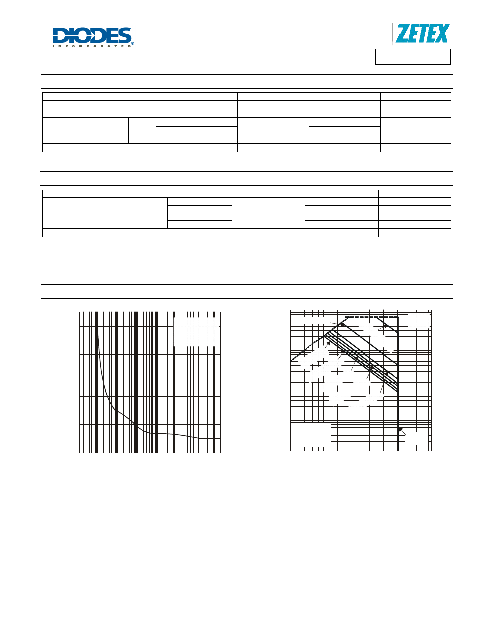
Thermal Characteristics
0
1
2
3
4
5
6
7
8
9
10
0.0001 0.001
0.01
0.1
1
10
100
1000
t1, PULSE DURATION TIME (sec)
Fig. 1 Single Pulse Maximum Power Dissipation
Single Pulse
R
= 136 C/W
θJA
°
R
(t) = R
*r(t)
T - T = P*R
θ
θ
θ
JA
JA
J
A
JA
P(
p
k
),
PEA
K
TRANS
IENT P
O
W
E
R
(W
)
0.1
1
10
100
V
, DRAIN-SOURCE VOLTAGE (V)
DS
Fig. 2 SOA, Safe Operation Area
0.01
0.1
1
10
I
, DRAI
N CURRENT
(
A
)
D
0.001
I (
A)
@
P
=1
0s
D
W
I (
A)
@
D
C
D
I (
A)
@
P
=1
s
D
W
I (
A)
@
P
=1
00
ms
D
W
I (
A)
@
P
=1
0m
s
D
W
T
= 150 C
T = 25 C
Single Pulse
J(MAX)
A
°
°
R
Limited
DS(ON)
I (A) @P =1ms
D
W
I (A) @
P =10µs
D
W
I
(A
) @
P
=1
00
µs
D
W