Diodes DMN2013UFDE User Manual
Dmn2013ufde, Product summary, Description
DMN2013UFDE
Document number: DS35701 Rev. 7 - 2
1 of 6
April 2013
© Diodes Incorporated
DMN2013UFDE
20V N-CHANNEL ENHANCEMENT MODE MOSFET
Product Summary
V
(BR)DSS
R
DS(ON) MAX
Package
I
D
T
A
= +25°C
20V
11m
@ V
GS
= 4.5V U-DFN2020-6 10.5A
13mΩ @ V
GS
= 2.5V U-DFN2020-6 9.4A
30m
@ V
GS
= 1.8V U-DFN2020-6 6.5A
50mΩ @ V
GS
= 1.5V U-DFN2020-6 5.5A
Description
This new generation MOSFET has been designed to minimize the on-
state resistance (R
DS(ON)
) and yet maintain superior switching
performance, making it ideal for high efficiency power management
applications.
Applications
General Purpose Interfacing Switch
Power Management Functions
Features
0.6mm profile – ideal for low profile applications
PCB footprint of 4mm
2
Low Gate Threshold Voltage
ESD
Protected
Gate
Totally Lead-Free & Fully RoHS Compliant (Notes 1 & 2)
Halogen and Antimony Free. “Green” Device (Note 3)
Qualified to AEC-Q101 Standards for High Reliability
PPAP Capable (Note 4)
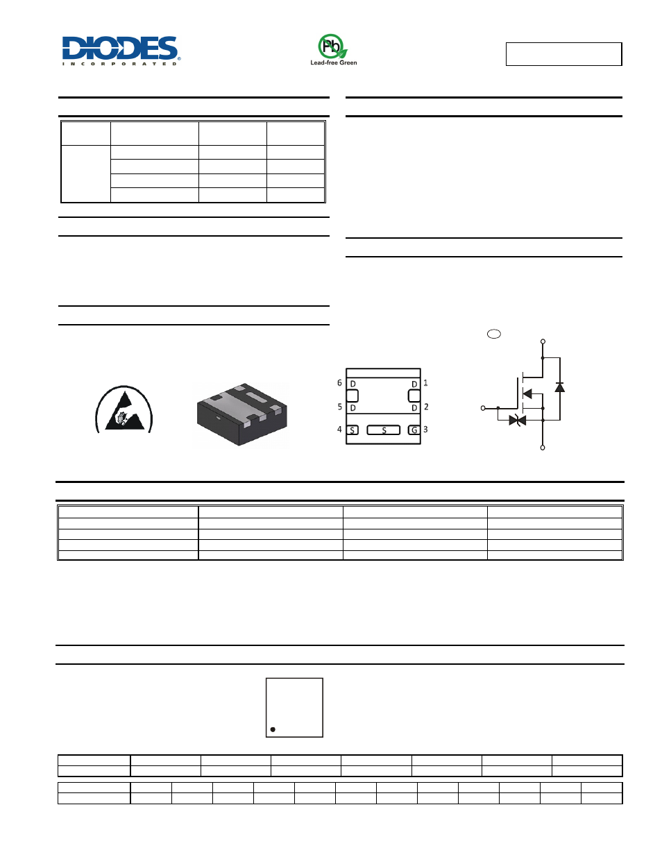
Mechanical Data
Case:
U-DFN2020-6
Case Material: Molded Plastic, “Green” Molding Compound. UL
Flammability Classification Rating 94V-0
Moisture Sensitivity: Level 1 per J-STD-020
Terminals: Finish – NiPdAu over Copper leadframe. Solderable
per MIL-STD-202, Method 208
Weight: 0.0065 grams (approximate)
Ordering Information
(Note 5)
Part Number
Compliance Case
Quantity per reel
DMN2013UFDE-7 Standard
U-DFN2020-6
3,000
DMN2013UFDEQ-7 Automotive
U-DFN2020-6
3,000
DMN2013UFDE-13 Standard
U-DFN2020-6
10,000
DMN2013UFDEQ-13 Automotive
U-DFN2020-6
10,000
Notes:
1. No purposely added lead. Fully EU Directive 2002/95/EC (RoHS) & 2011/65/EU (RoHS 2) compliant.
2. S more information about Diodes Incorporated’s definitions of Halogen- and Antimony-free, "Green"
and Lead-free.
3. Halogen- and Antimony-free "Green” products are defined as those which contain <900ppm bromine, <900ppm chlorine (<1500ppm total Br + Cl) and
<1000ppm antimony compounds.
4. Automotive products are AEC-Q101 qualified and are PPAP capable. Automotive, AEC-Q101 and standard products are electrically and thermally the
same, except where specified. For more information, please refer
5. For packaging details, go to our website at http”
Marking Information
Date Code Key
Year
2011
2012
2013
2014
2015
2016
2017
Code Y Z A B C D E
Month
Jan
Feb
Mar
Apr
May
Jun
Jul
Aug
Sep
Oct
Nov
Dec
Code 1 2 3 4 5 6 7 8 9 O N D
U-DFN2020-6
Bottom View
Pin Out
ESD PROTECTED
Equivalent Circuit
Source
Gate
Protection
Diode
Gate
Drain
N6 = Product Type Marking Code
YM = Date Code Marking
Y = Year (ex: Y = 2011)
M = Month (ex: 9 = September)
N6
YM
e4