Maximum ratings, Thermal characteristics, Electrical characteristics – Diodes DMN2004K User Manual
Page 2: Dmn2004k
DMN2004K
Document number: DS30938 Rev. 9 - 2
2 of 6
July 2013
© Diodes Incorporated
DMN2004K
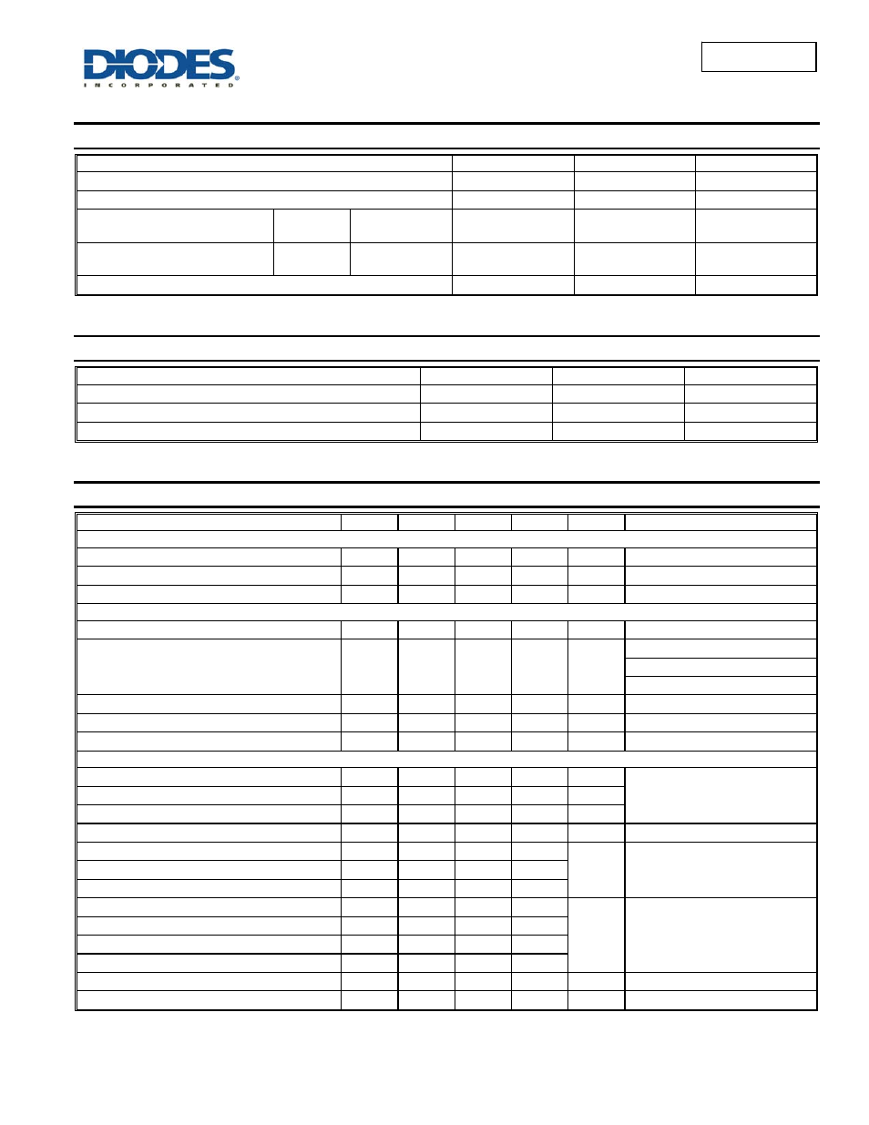
Maximum Ratings
(@T
A
= +25°C, unless otherwise specified.)
Characteristic Symbol
Value
Units
Drain-Source Voltage
V
DSS
20 V
Gate-Source Voltage
V
GSS
±8 V
Drain Current (Note 5) V
GS
= 4.5V
Steady
State
T
A
= +25°C
T
A
= +85°C
I
D
630
450
mA
Drain Current (Note 5) V
GS
= 1.8V
Steady
State
T
A
= +25°C
T
A
= +85°C
I
D
410
300
mA
Pulsed Drain Current (Note 6)
I
DM
1.5 A
Thermal Characteristics
(@T
A
= +25°C, unless otherwise specified.)
Characteristic Symbol
Value
Units
Total Power Dissipation (Note 5)
P
D
350 mW
Thermal Resistance, Junction to Ambient
R
θJA
357 °C/W
Operating and Storage Temperature Range
T
J,
T
STG
-65 to +150
°C
Electrical Characteristics
(@T
A
= +25°C, unless otherwise specified.)
Characteristic Symbol
Min
Typ
Max
Unit
Test
Condition
OFF CHARACTERISTICS (Note 7)
Drain-Source Breakdown Voltage
BV
DSS
20
V
V
GS
= 0V, I
D
= 10µA
Zero Gate Voltage Drain Current
I
DSS
1 µA
V
DS
= 16V, V
GS
= 0V
Gate-Source Leakage
I
GSS
1
µA
V
GS
=
4.5V, V
DS
= 0V
ON CHARACTERISTICS (Note 7)
Gate Threshold Voltage
V
GS(th)
0.5
1.0 V
V
DS
= V
GS
, I
D
= 250µA
Static Drain-Source On-Resistance
R
DS(ON)
0.4
0.5
0.7
0.55
0.70
0.9
Ω
V
GS
= 4.5V, I
D
= 540mA
V
GS
= 2.5V, I
D
= 500mA
V
GS
= 1.8V, I
D
= 350mA
Forward Transfer Admittance
|Y
fs
|
200
ms
V
DS
=10V, I
D
= 0.2A
Source Current
I
S
0.5 A
Diode Forward Voltage (Note 7)
V
SD
0.6
1 V
V
GS
= 0V, I
S
= 500mA
DYNAMIC CHARACTERISTICS
Input Capacitance
C
iss
150 pF
V
DS
= 16V, V
GS
= 0V
f = 1.0MHz
Output Capacitance
C
oss
25 pF
Reverse Transfer Capacitance
C
rss
20 pF
Gate Resistance
R
g
292
Ω
V
DS
= 0V, V
GS
= 0V, f = 1.0MHz
Total Gate Charge
Q
g
0.9
nC
V
DS
= 15V, V
GS
= 4.5V, I
D
= 0.5A
Gate-Source Charge
Q
gs
0.2
Gate-Drain Charge
Q
gd
0.2
Turn-On Delay Time
t
D(on)
5.7
ns
V
GS
= 8V, V
DS
= 15V,
R
G
= 6
, R
L
= 30
Turn-On Rise Time
t
r
8.4
Turn-Off Delay Time
t
D(off)
59.4
Turn-Off Fall Time
t
f
37.6
Body Diode Reverse Recovery Time
t
rr
5.5
ns
I
S
= 0.5A, dI/dt = -100A/µs
Body Diode Reverse Recovery Charge
Q
rr
0.85
nC
I
S
= 0.5A, dI/dt = -100A/µs
Notes:
5. Device mounted on FR-4 PCB, with minimum recommended pad layout, single sided.
6. Pulse width
≤10µS, Duty Cycle ≤1%.
7. Short duration pulse test used to minimize self-heating effect.