Dxt651, Maximum ratings, Thermal characteristics – Diodes DXT651 User Manual
Page 2: Thermal characteristics and derating information, Derating curve, Transient thermal impedance, Pulse power dissipation
DXT651
Document Number: DS31184 Rev: 5 - 2
2 of 6
February 2013
© Diodes Incorporated
DXT651
Maximum Ratings
(@T
A
= +25°C, unless otherwise specified.)
Characteristic Symbol
Value
Unit
Collector-Base Voltage
V
CBO
80 V
Collector-Emitter Voltage
V
CEO
60 V
Emitter-Base Voltage
V
EBO
5 V
Collector Current
I
C
3 A
Peak Pulse Collector Current
I
CM
6 A
Base Current
I
B
500 mA
Thermal Characteristics
(@T
A
= +25°C, unless otherwise specified.)
Characteristic Symbol
Value
Unit
Power Dissipation (Note 5)
P
D
1 W
Thermal Resistance, Junction to Ambient Air (Note 5)
R
θJA
125 °C/W
Thermal Resistance, Junction to Leads (Note 6)
R
θJL
18.2 °C/W
Operating and Storage Temperature Range
T
J
, T
STG
-55 to +150
°C
Notes:
5. For a device surface mounted on 25mm X 25mm FR4 PCB with high coverage of single sided 1 oz copper, in still air conditions; the device is measured
when operating in a steady-state condition.
6. Thermal resistance from junction to solder-point (on the exposed collector pad).
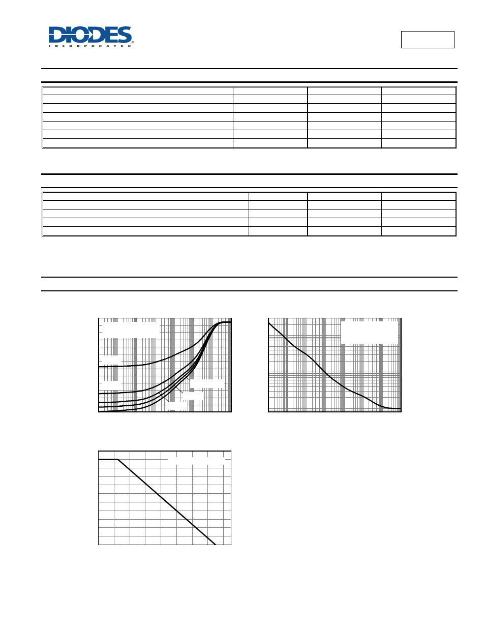
Thermal Characteristics and Derating Information
0
20
40
60
80
100 120 140 160
0.0
0.2
0.4
0.6
0.8
1.0
25mm x 25mm 1oz Cu
Derating Curve
Temperature (°C)
M
a
x
P
o
wer
Di
s
s
ipat
ion (
W
)
100µ
1m
10m 100m
1
10
100
1k
0
20
40
60
80
100
120
25mm x 25mm 1oz Cu
T
amb
=
25°C
Transient Thermal Impedance
D=0.5
D=0.2
D=0.1
Single Pulse
D=0.05
T
her
m
a
l Res
is
tanc
e (°
C/
W
)
Pulse Width (s)
100µ
1m
10m 100m
1
10
100
1k
1
10
100
25mm x 25mm 1oz Cu
T
amb
=
25°C
Single pulse
Pulse Power Dissipation
Pulse Width (s)
M
a
x
P
o
wer
D
is
s
ipat
ion (
W
)