Mbr3100, Marking information, Maximum ratings – Diodes MBR3100 User Manual
Page 3
MBR3100
Document number: DS36956 Rev. 1 - 2
3 of 9
June 2014
© Diodes Incorporated
MBR3100
Marking Information
(Cont.)
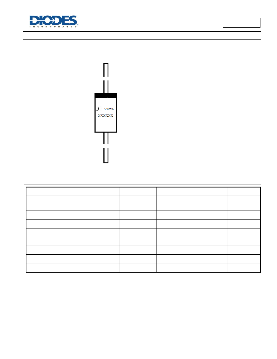
(2) DO-27
(Top View)
Maximum Ratings
(Note 5)
Characteristic
Symbol
Rating
Unit
Peak Repetitive Reverse Voltage
Working Peak Reverse Voltage
DC Blocking Voltage
V
RRM
V
RWM
V
R
100
V
Average Rectified Forward Current (Rated V
R
, T
C
=
+141
C)
I
F(AV)
3
A
Non Repetitive Peak Surge Current (Surge Applied at
Rated Load Conditions Half Wave, Single Phase, 60Hz)
I
FSM
80
A
Operating Junction Temperature Range (Note 6)
T
J
-65 to +150
C
Storage Temperature Range
T
STG
-65 to +150
C
Voltage Rate of Change (Rated V
R
)
dv/dt
10000
V/µs
ESD (Machine Model = C)
–
400
V
ESD (Human Body Model = 3B)
–
8000
V
Notes: 5.
Stresses greater than those listed under “Absolute Maximum Ratings” may cause permanent damage to the device. These are stress ratings only, and
functional operation of the device at these or any other conditions beyond those indicated under “Recommended Operating Conditions” is not implied.
Exposure to “Absolute Maximum Ratings” for extended periods may affect device reliability.
6. The heat generated must be less than the thermal conductivity from Junction to Ambient: dP
D
/dT
J
< 1/
θ
JA
.
First Line: Logo and Date Code
Y: Year
WW: Work Week of Molding
A: Assembly House Code
Second Line: Marking ID
(See Ordering Information)