Diodes AZ75232 User Manual
Page 4
4
Oct. 2009 Rev. 1. 7
BCD Semiconductor Manufacturing Limited
Data Sheet
MULTIPLE RS-232 DRIVERS AND RECEIVERS AZ75232
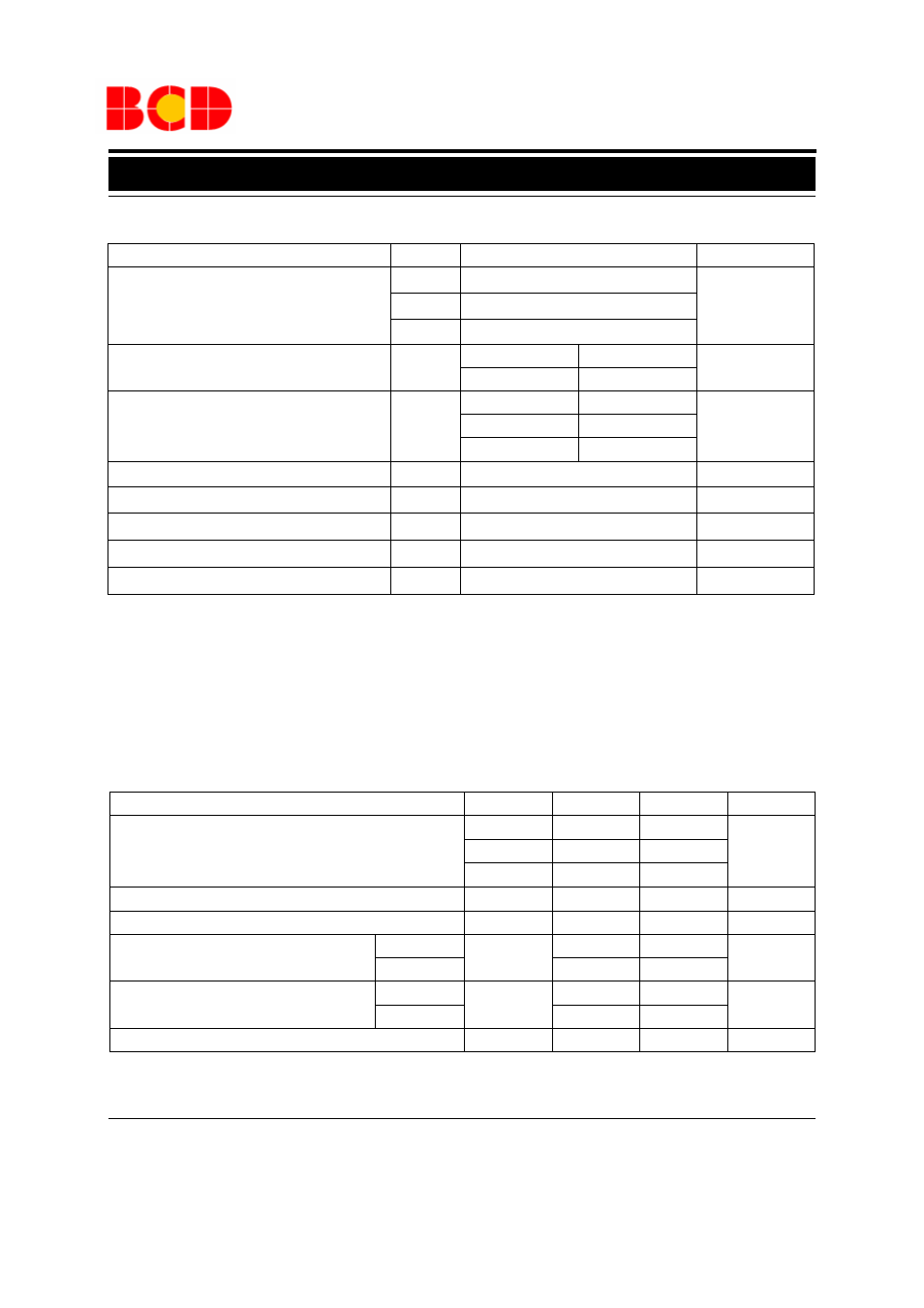
Parameter Symbol
Value
Unit
Supply Voltage
V
DD
15
V
V
SS
-15
V
CC
7
Input Voltage Range
V
I
Driver
-15 to 7
V
Receiver
-30 to 30
Power Dissipation (T
A
=25
o
C)
P
D
SOIC-20
1340
mW
SSOP-20
1210
TSSOP-20
1100
Driver Output Voltage Range
V
O
-15 to 15
V
Receiver Low-Level Output Current
I
OL
20
mA
Operating Junction Temperature
T
J
150
o
C
Storage Temperature Range
T
STG
-65 to 150
o
C
Lead Temperature (Soldering, 10sec)
T
LEAD
260
o
C
Note 1: Stresses greater than those listed under "Absolute Maximum Ratings" may cause permanent damage to the device.
These are stress ratings only, and functional operation of the device at these or any other conditions beyond those indicated
under "Recommended Operating Conditions" is not implied. Exposure to "Absolute Maximum Ratings" for extended periods
may affect device reliability.
Parameter
Symbol
Min
Max
Unit
Supply Voltage
V
DD
7.5
15
V
V
SS
-15
-7.5
V
CC
4.5
5.5
High-Level Input Voltage (Driver Only)
V
IH
1.9
V
Low-Level Input Voltage (Driver Only)
V
IL
0.8
V
High-Level Output Current
Driver
I
OH
-6
mA
Receiver
-0.5
Low-Level Output Current
Driver
I
OL
6
mA
Receiver
16
Operating Temperature Range
T
A
-40
85
o
C
Recommended Operating Conditions
Absolute Maximum Ratings (Note 1)