Voltage detector az70xx data sheet, Electrical characteristics – Diodes AZ70XX User Manual
Page 5
5
BCD Semiconductor Manufacturing Limited
VOLTAGE DETECTOR AZ70XX
Data Sheet
Oct. 2011 Rev. 2. 2
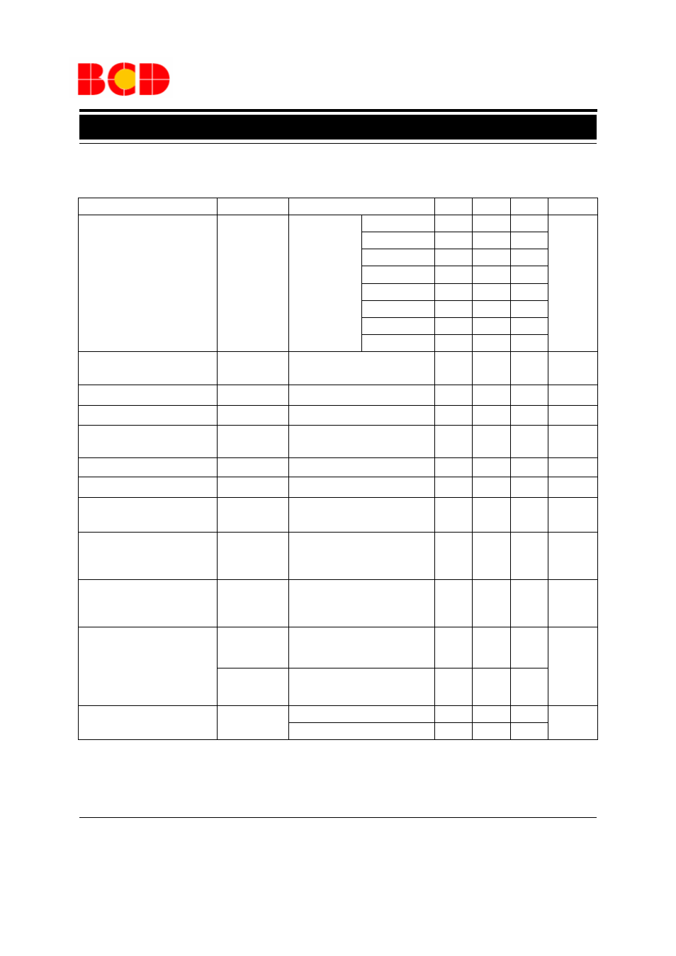
Parameter
Symbol
Conditions
Min
Typ
Max
Unit
Detect
Voltage
V
DET
R
L
=200
Ω
(Note 2)
V
OL
≤
0.4V
AZ7023R/Z
2.15
2.3
2.45
V
AZ7025R/Z
2.35
2.5
2.65
AZ7027R/Z
2.55
2.7
2.85
AZ7029R/Z
2.75
2.9
3.05
AZ7031R/Z
2.95
3.1
3.25
AZ7033R/Z
3.15
3.3
3.45
AZ7042R/Z
4.05
4.2
4.35
AZ7045R/Z
4.35
4.5
4.65
Low-level Output Voltage
V
OL
V
CC
=V
DET
(min)-0.05V
R
L
=200
Ω (Note 2)
0.4
V
Output Leakage Current
I
OH
V
CC
=18V
0.1
µA
Hysteresis Voltage
V
HYS
R
L
=200
Ω (Note 2)
30
50
100
mV
Detect Voltage Temperature
Coefficient
∆V
DET
/(V
DET
×
∆T)
R
L
=200
Ω (Note 2)
±0.01
% /
o
C
Circuit Current at On Time
I
CCL
V
CC
=V
DET
(min)-0.05V
300
500
µA
Circuit Current at Off Time
I
CCH
V
CC
=5.25V
30
50
µA
Minimum Operating Voltage
V
OPR
R
L
=200
Ω (Note 2)
V
OL
≤
0.4V
0.8
V
“
L” Transmission Delay Time
tpHL
V
CC
changed from 5.25V to
V
DET
(min)-0.05V, R
L
=1.0K
Ω,
C
L
=100p (Note 3)
10
µs
“
H” Transmission Delay Time
tpLH
V
CC
changed from V
DET
(min)-
0.05V to 5.25V, R
L
=1.0K
Ω,
C
L
=100p (Note 3)
15
µs
Output Current at On Time
I
OL
Ⅰ
V
CC
=V
DET
(min)-0.05V
T
A
=25
o
C (Note 4)
20
mA
I
OL
Ⅱ
V
CC
=V
DET
(min)-0.05V
T
A
=-40 to 85
o
C (Note 4)
16
Thermal Resistance
(Junction to Case)
θ
JC
TO-92
72
o
C/W
SOT-89
74
Electrical Characteristics
T
A
=25
o
C, unless otherwise specified.
Note 2: See test circuit 1 and Figure 12.
Note 3: See test circuit 2 and Figure 12.
Note 4: See test circuit 3. Adjusting the regulative power source until the reading value of voltage meter V is 0.4V, the reading
value of current meter A is defined as "Output Current at On Time".