Diodes AZ78LXX User Manual
Page 6
3-TERMINAL POSITIVE LINEAR REGULATOR AZ78LXX
Data Sheet
6
Nov. 2012 Rev. 2. 2
BCD Semiconductor Manufacturing Limited
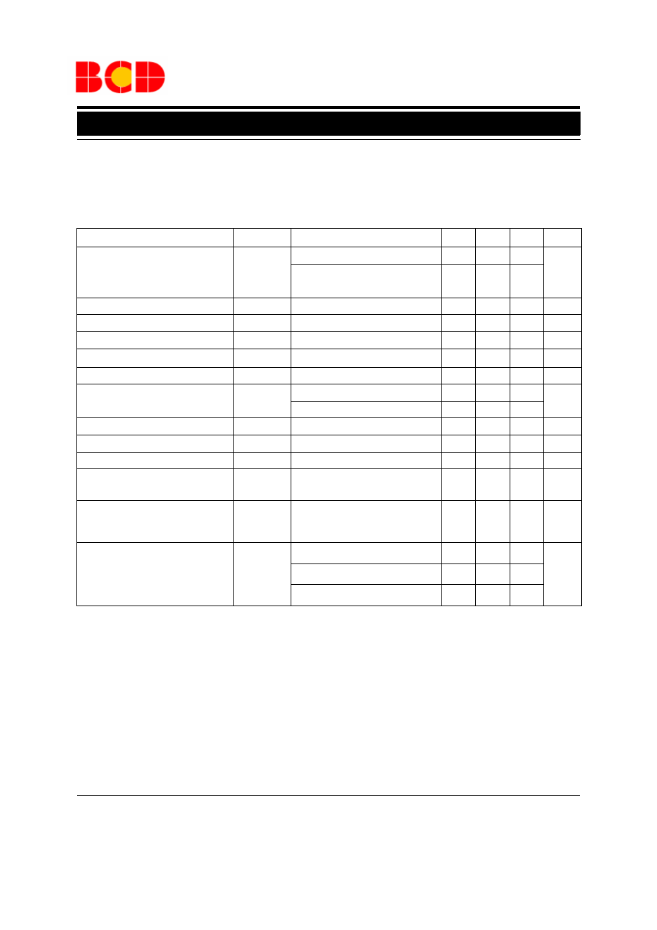
Parameter
Symbol
Conditions
Min
Typ
Max
Unit
Output Voltage
V
OUT
4.8
5
5.2
V
7.0V ≤ V
IN
≤
15V
1.0mA ≤ I
OUT
≤
40mA (Note 2)
4.75
5.25
Line Regulation
V
RLINE
7.0V ≤ V
IN
≤
15V
18
75
mV
Load Regulation
V
RLOAD
1.0mA ≤ I
OUT
≤
100mA
20
60
mV
Dropout Voltage
V
DROP
1.6
V
Current Limit
I
LIMIT
T
J
=25
o
C
150
mA
Quiescent Current
I
Q
I
OUT
=0
3
5
mA
Quiescent Current Change
ΔI
Q
8.0V ≤ V
IN
≤
15V
1.0
mA
1.0mA ≤ I
OUT
≤
40mA
0.1
Output Noise Voltage
N
O
10Hz ≤ f ≤ 100kHz (Note 3)
40
μV
Ripple Rejection
PSRR
f=120Hz, 8.0V ≤ V
IN
≤
15V
47
62
dB
Peak Output Current
I
PK
150
mA
Average Temperature Coefficient of
Output Voltage
ΔV
OUT
/
ΔT I
OUT
= 5.0mA
0.65
mV/
o
C
Minimum Value of Input Voltage
Required to Maintain Line Regula-
tion
V
IN
(Min)
6.7
7
V
Thermal Resistance
θ
JC
TO-92
81
o
C/W
SOT-89
29.8
SOT-223
71
Limits in standard typeface are for T
J
=25
o
C
, Bold typeface applies over -40
o
C
to 125
o
C,
I
OUT
=40mA, C
IN
=0.33
μ
F, C
OUT
=0.1
μ
F, V
IN
=10V, unless otherwise specified.
Note 2: Power Dissipation ≤ 0.6W
Note 3: Recommended minimum load capacitance of 0.01
μF to limit high frequency noise.
AZ78L05 Electrical Characteristics
Electrical Characteristics